
Professional PCB manufacturing and assembly
Building 6, Zone 3, Yuekang Road,Bao'an District, Shenzhen, China
+86-13410863085Mon.-Sat.08:00-20:00


How much is the salary of PCB design engineers?
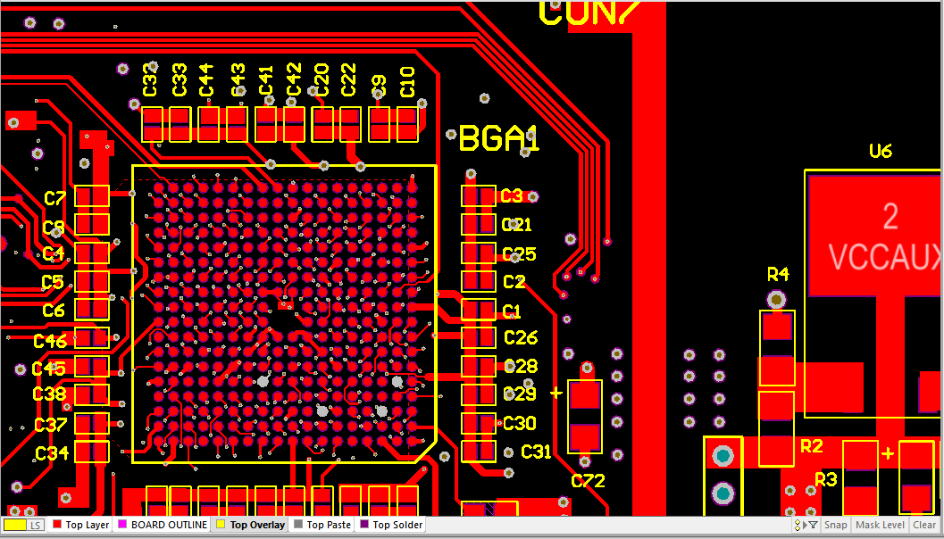
PCB design is based on circuit schematic diagram to realize specific functions on PCB. PCB design should take into account layout design, external connection layout, optimal layout of internal electronic components and other factors. The function of PCB design is to standardize design operations, improve production efficiency and improve the quality of electronic products.
Data required for PCB design:
1. Schematic diagram: it can generate correct netlist in complete electronic document format, and provide the layout and functions required by PCB
2. Mechanical dimensions: provide PCB with multiple physical information such as specific location and direction identification of electronic components
3. Device packaging: provide device packaging library, packaging method and electronic material specification for PCB
4. Wiring guide: provide PCB with specific requirements description of special signals, impedance and other designs
The salary of PCB design engineers is closely related to their actual working ability. According to different abilities, thousands of yuan of salary per month to millions of yuan of annual salary exist.
Proportion of PCB design engineers' salary distribution:
1. Below 4K: 20.0% of the total
2. 4K-6K: 12.0% of the total
3. 6K-8K: 24.0% of the total
4. 8K-10K: 16.0% of the total
5. 10K-15K: 18.0% of the total
6. Other salary range: 10.0% of the total
According to the data of recruitment websites such as 58 cities, Boss direct employment and 51job, the monthly salary of 6K-15K is a large proportion. Accounting for 58% of the total population.
The salary of entry-level PCB design engineers is generally less than 4K. They are mainly fresh college graduates who can be familiar with the basic knowledge of PCB design and can independently complete the conventional PCB design of 2-layer boards.
The salary of junior engineers is generally 4K-6K, and the working years are about 1-2 years. They can independently complete the conventional PCB design of 2-4 layers of boards, and can complete the detailed PCB design and PCB proofing test verification under the guidance.
The salary of intermediate engineers is generally 6-10K, and the working years are about 2-4 years. They can independently complete the design of 2-6 layers of conventional PCB, have a general understanding of conventional high-speed PCB design, and independently complete the detailed design of PCB and PCB proofing test verification.
The salary of senior engineer is generally 10-15K, and the working years are 3-5 years. He is proficient in 2-12-layer PCB design, can complete high-speed (DDR series design) and high-density (HDI design) PCB design, leads the completion of PCB detailed design and PCB proofing test verification, and can participate in the completion of PCB overall design.
The salary of the super engineer is generally 15-30K. He is proficient in high-speed and high-density PCB design, can complete IC design, and can lead the work of product demand and overall design.
Although the entry threshold for PCB design engineers is low, there is a lot of room for improvement. The software to be proficient in includes AD, Allegro, PADS, layout, SI, PI, EMC, etc. Only when they become senior experts in one position can their income be more objective.
Are there any skills in high-speed PCB design?
Oct 27,2022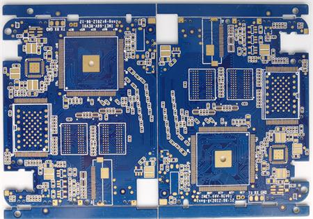


Just upload Gerber files, BOM files and design files, and the KINGFORD team will provide a complete quotation within 24h.