
Professional PCB manufacturing and assembly
Building 6, Zone 3, Yuekang Road,Bao'an District, Shenzhen, China
+86-13410863085Mon.-Sat.08:00-20:00


What are the precautions for PCB component layout?
In the PCB manufacturing process, component layout is an important part. Improper placement will cause circuit compatibility problems and signal integrity problems, which will lead to the failure of PCB design. So, what are the precautions for PCB component layout?
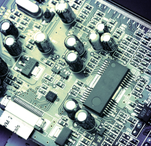
Layout of PCB components
1. On the premise of ensuring the electrical performance, the components shall be placed on the grid and parallel or vertical to each other, so as to be neat and beautiful. In general, overlapping is not allowed; The components and parts shall be arranged compactly, and shall be distributed evenly and uniformly throughout the layout.
2. In general, all components shall be arranged on the same side of; Only when the top layer components are too dense, can some components with limited height and low heat generation, such as chip resistance, chip capacitor, chip IC, be placed in the lower layer.

3. Take the core components of each functional unit as the center, and arrange around it; Try to reduce and shorten the lead wires and connections between components.
4. The distance between components and PCB edge is generally not less than 2MM.
5. The minimum spacing between different components shall be more than 1MM.
6. For circuits operating at high frequencies, the distribution parameters between components should be considered.
7. The location of special components needs to be carefully analyzed. First, determine the size of PCB, and then determine the placement position of special components; Finally, all components of the circuit are arranged according to the functional unit.
8. Inspection of component layout:
(1) Whether the dimensions conform to the drawing requirements.
(2) Whether there are conflicts at all levels. Such as whether the components, frames, and layers requiring private printing are reasonable.
(3) Whether the layout of components is balanced and orderly, and whether they have been completely distributed.
(4) Whether the heat dissipation is good.
(5) Whether the distance between thermal components and heating components is reasonable.
(6) Whether the interference of the line needs to be considered.
(7) Whether the commonly used components are convenient for use.
The above is the explanation given by the editor of pcb circuit board company. If you want to know more about PCBA, you can go to our company's home page to learn about it. In addition, our company also sells various circuit boards,
High frequency circuit board and SMT chip are waiting for your presence again.


Just upload Gerber files, BOM files and design files, and the KINGFORD team will provide a complete quotation within 24h.