
Professional PCB manufacturing and assembly
Building 6, Zone 3, Yuekang Road,Bao'an District, Shenzhen, China
+86-13410863085Mon.-Sat.08:00-20:00

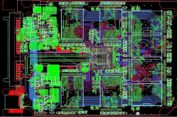
In PCB design, it is necessary to pay attention to EMI, EMC, SI, PI and other factors. In PCB design, anti-interference requirements should be fully considered and met. There are three basic elements of interference:
(1) Interference source refers to the component, equipment or signal that generates interference. It is described in mathematical language as follows: du/dt, where di/dt is large, is the interference source. For example, lightning, relay, silicon controlled rectifier, motor, high-frequency clock, etc. may become interference sources.
(2) Propagation path refers to the path or medium through which interference propagates from the interference source to the sensitive device. The typical interference propagation path is conducted through wires and radiated from space.

(3) Sensitive devices refer to objects that are easy to be interfered with. Such as: A/D, D/A converter, microcontroller, digital IC, weak signal amplifier, etc.
The basic principle of anti-interference design is to restrain the interference source, cut off the interference propagation path and improve the anti-interference performance of the sensitive device. (Similar to the prevention of infectious diseases)
1 Suppress interference sources - Suppressing interference sources is to reduce du/dt, di/dt of interference sources as much as possible. This is the most priority and most important principle in anti-interference design, which can often achieve twice the result with half the effort. The du/dt of the interference source is reduced mainly by paralleling capacitors at both ends of the interference source. The di/dt of the interference source is reduced by adding inductance or resistance in series and freewheeling diode in the interference source circuit. Common measures to suppress interference sources are as follows:
(1) The relay coil is added with a freewheeling diode to eliminate the back EMF interference generated when the coil is disconnected. Only adding freewheeling diode will delay the disconnection time of the relay, and the relay can act more times in a unit time after adding voltage stabilizing diode.
(2) Connect the spark suppression circuit at both ends of the relay contact in parallel (generally RC series circuit, with a resistance of K to tens of K and a capacitance of 0.01uF) to reduce the impact of electric spark.
(3) Add a filter circuit to the motor, and pay attention to the capacitor and inductor leads should be as short as possible.
(4) Each IC on the circuit board shall be connected to 0.01 in parallel μ F~0.1 μ F High frequency capacitor to reduce the influence of IC on power supply. Pay attention to the wiring of high-frequency capacitor. The wiring should be close to the power terminal and as short as possible. Otherwise, the equivalent series resistance of the capacitor will be increased, which will affect the filtering effect.
(5) Avoid 90 degree polyline during wiring to reduce high-frequency noise emission.
(6) The RC suppression circuit is connected at both ends of the thyristor in parallel to reduce the noise generated by the thyristor (when the noise is serious, the thyristor may be broken down). According to the propagation path of interference, it can be divided into conducted interference and radiated interference. The so-called conducted interference refers to the interference transmitted to the sensitive device through the wire. The frequency band of high-frequency interference noise is different from that of useful signal. The transmission of high-frequency interference noise can be cut off by adding a filter on the wire. Sometimes, isolation optocouplers can be added to solve this problem. Power supply noise is the most harmful, so special attention should be paid to handling. The so-called radiation interference refers to the interference transmitted to sensitive devices through space radiation. The general solution is to increase the distance between the interference source and the sensitive device, isolate them with a ground wire and add a shield on the sensitive device.
2 Common measures to cut off interference propagation path are as follows:
(1) Fully consider the influence of power supply on MCU. If the power supply is well done, the anti-interference of the whole circuit will be more than half solved. Many single chip computers are very sensitive to power supply noise. To reduce the interference of power supply noise to single chip computers, filter circuits or voltage regulators should be added to the power supply of single chip computers. For example, magnetic beads and capacitors can be used to form a π - shaped filter circuit. Of course, 100 Ω resistors can also be used to replace magnetic beads when conditions are not demanding.
(2) If the I/O port of the single chip microcomputer is used to control noise devices such as motors, isolation shall be added between the I/O port and the noise source (π filtering circuit shall be added). To control noise devices such as motor, isolation shall be added between I/O port and noise source (π filtering circuit shall be added).
(3) Pay attention to crystal oscillator wiring. The crystal oscillator shall be as close as possible to the pin of the microcontroller, and the clock area shall be isolated by the ground wire. The crystal oscillator shell shall be grounded and fixed. This measure can solve many difficult problems.
(4) The circuit board shall be reasonably partitioned, such as strong and weak signals, digital and analog signals. Try to keep the interference sources (such as motors and relays) away from the sensitive elements (such as SCM).
(5) The digital area shall be isolated from the analog area with a ground wire. The digital ground shall be separated from the analog ground, and finally connected to the power supply ground at one point. The wiring of A/D and D/A chips is also based on this principle. The manufacturer has considered this requirement when allocating the pin arrangement of A/D and D/A chips.
(6) The ground wire of single chip microcomputer and high-power device shall be grounded separately to reduce mutual interference. High power devices shall be placed on the edge of the circuit board as far as possible.
(7) Anti interference components such as magnetic beads, magnetic rings, power filters and shielding covers are used in the I/O ports, power lines, circuit board connecting lines and other key areas of the microcontroller, which can significantly improve the anti-interference performance of the circuit.
3 Improving the anti-interference performance of sensitive devices Improving the anti-interference performance of sensitive devices refers to the method of minimizing the pickup of interference noise from the sensitive devices and recovering from abnormal conditions as soon as possible. Common measures to improve the anti-interference performance of sensitive devices are as follows:
(1) The area of the loop shall be minimized during PCB wiring to reduce the induced noise.
(2) When wiring PCB, the power line and ground wire should be as thick as possible. In addition to reducing the voltage drop, it is more important to reduce the coupling noise.
(3) For the idle I/O port of the microcontroller, do not hang in the air, but ground or connect to the power supply. The idle terminals of other ICs are grounded or connected to the power supply without changing the system logic.
(4) The use of power supply monitoring and watchdog circuits for SCM, such as IMP809, IMP706, IMP813, X25043, X25045, can greatly improve the anti-interference performance of the entire circuit.
(5) On the premise that the speed can meet the requirements, the crystal oscillator of the single chip microcomputer shall be reduced as far as possible and the low-speed digital circuit shall be selected.
(6) IC devices shall be directly welded to the circuit board as much as possible, and IC sockets shall be used less.
PCB design software:
1. It is used to clearing all unused code spaces to "0", because this is equivalent to NOP, which can be returned when the program runs;
2. Add several NOPs before the jump instruction, with the same purpose as 1; 3. When there is no hardware WatchDog, software can be used to simulate the WatchDog to monitor the operation of the program;
4. When dealing with the parameter adjustment or setting of external devices, the parameters can be re sent regularly to prevent the external devices from making errors due to interference, so that the external devices can recover correctly as soon as possible;
5. For anti-interference in communication, the data check bit can be added, and the two out of three or three out of five strategy can be adopted; 6. When there are communication lines, such as I ^ 2C, three wire system, etc., in practice, we find that the data line, CLK line and INH line are normally set to high, and their anti-interference effect is better than low.
Hardware:
1. The part line of ground wire and power line must be important!
2. Decoupling of lines;
3. Separation of digital and analog ground;
4. Each digital element needs 104 capacitors between the ground and the power supply;
5. In relay applications, especially when there is a large current, to prevent the interference of relay contact sparks on the circuit, a 104 and a diode can be connected between the relay coils, and 472 capacitors can be indirectly connected between the contact and the normal starting point. The effect is good!
6. To prevent crosstalk of I/O ports, I/O ports can be isolated by diode isolation, gate circuit isolation, optocoupler isolation, electromagnetic isolation, etc;
7. Of course, the anti-interference of PCB multilayer board is certainly better than that of single panel, but the cost is several times higher.
8. Choosing a device with strong anti-interference ability is more effective than any other method, because the inherent shortcomings of the device are difficult to be remedied by external methods.
This paper mainly introduces EMI, EMC, SI, PI and other factors in PCB design

What design principles should PCB follow?
Oct 22,2022


Just upload Gerber files, BOM files and design files, and the KINGFORD team will provide a complete quotation within 24h.