
Professional PCB manufacturing and assembly
Building 6, Zone 3, Yuekang Road,Bao'an District, Shenzhen, China
+86-13410863085Mon.-Sat.08:00-20:00

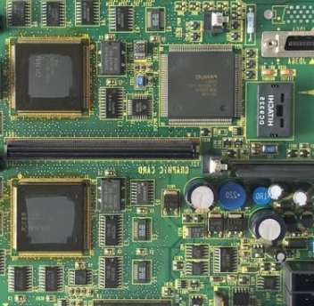
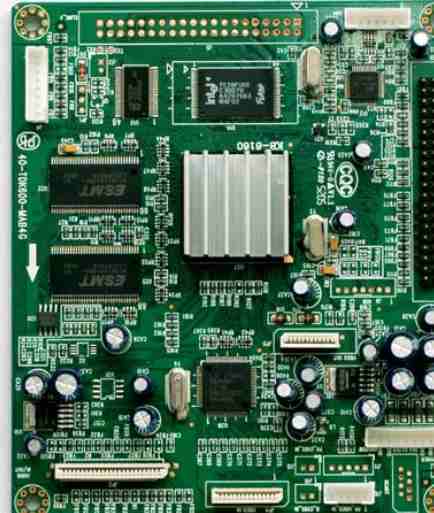
Shenzhen kingford is a professional PCB design company engaged in electronic products layout layout design, mainly undertake multi-layer, high density PCB design and circuit board design proofing business. PCB design layout is very important, good layout can achieve twice the result with half the effort, the next for you to introduce the PCB design layout ideas and principles.
1. First of all, we will place the device with the required structure. When placing, according to the structure of the import, the connector must pay attention to the position of pin 1.
2, PCB design layout should pay attention to the structure of the height limit requirements.
3, if the PCB design layout is beautiful, generally according to the component frame or center line coordinates to position (center alignment).
4, the overall PCB design layout should consider heat dissipation.
5, PCB design and layout need to consider the wiring channel evaluation, consider the space required by the same length.
6, PCB design layout needs to consider the power flow direction, evaluate the power channel.
7, high speed, medium speed, low speed circuit to separate.
8, strong current, high voltage, strong radiation components away from weak current, low voltage, sensitive components.
9, analog, digital, power supply, protection circuit to separate.
10, the interface protection device should be placed as close to the interface as possible.
11. Placing sequence requirements of interface protection devices:
(1) The order of general power supply lightning protection devices is: varistor, fuse, diode suppression, EMI filter, inductance or common-mode inductance, for schematic absence of any device layout;
(2) The general order of protection devices for interface signals is: ESD(TVS tube), isolation transformer, common-mode inductance, capacitance, resistance, for the schematic loss of any device layout; Strictly follow the order of the schematics (with the ability to judge whether the schematics are correct) to lay out the "font" layout.
12. The level conversion chip (such as RS232) is placed close to the connector (such as serial port).
13. Keep devices susceptible to ESD interference, such as NMOS and CMOS devices, away from areas susceptible to ESD interference (such as the edge of a board).
14. PCB design and layout of clock devices:
(1) The crystal, crystal oscillator and clock distributor should be as close to the relevant IC devices as possible;
(2) The filter of the clock circuit (if possible, the filter of the "∏" type) should be close to the power input pin of the clock circuit;
(3) Whether the output of crystal oscillator and clock distributor is connected with a 22 ohm resistor;
(4) Whether the useless output pin of the clock distributor is grounded through the resistance;
(5) The PCB design layout of crystal, crystal oscillator and clock distributor should be far away from high-power components, radiators and other heating devices;
(6) Whether the distance between crystal vibration and plate edge and interface device is greater than 1inch.
15. Whether the switching power supply is far away from the AD/DA converter, simulator, sensitive device and clock device.
16. PCB design layout of switching power supply should be compact, input/output should be separated, PCB design layout should be carried out in strict accordance with the requirements of the schematic diagram, and capacitor of switching power supply should not be placed at will.
17. Capacitor and filter parts:
(1) The capacitor must be placed close to the power pin, and the smaller the capacitance value, the closer to the power pin;
(2) The EMI filter should be close to the input port of the chip power supply;
(3) In principle, a 0.1uF small capacitor for each power pin and one or more 10uF large capacitors for an integrated circuit can be increased or decreased according to specific circumstances

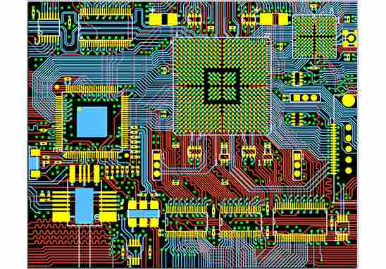
2. Golden Rule of PCB wiring
Shenzhen kingford is a professional PCB design company engaged in electronic products layout layout design, mainly undertake multi-layer, high density PCB design and circuit board design proofing business. Next, I will share the golden rule of PCB wiring.
PCB wiring is based on PCB circuit schematic diagram, wire table, and required wire width and spacing. Wiring should comply with the following rules:
1. On the premise of meeting the requirements of use, wiring should be as simple as possible. The order of selecting wiring mode is single-layer - double-layer - multilayer.
2. The wire layout between the two patch connecting disks should be as short as possible. Sensitive signals and small signals should go first to reduce the delay and interference of small signals. The input line of the analog circuit should be equipped with a ground wire shield; The wiring of the same layer should be evenly distributed; The conductive area on each layer should be relatively balanced to prevent the PCB warping in pcba processing.
3. The direction of the signal line should be oblique or smooth transition, and the radius of curvature is larger, to avoid electric field concentration, signal reflection and additional impedance.
4. Digital circuit and analog circuit should be separated on the wiring, so as not to dry each other, such as in the same layer should be the two circuits of the ground system and the power system of the wire separately laid, different frequency signal lines should be laid in the middle of the ground wire separated, avoid crosstalk. In order to test convenience, the design should set necessary breakpoints and test points.
5. When circuit components are grounded and connected to the power supply, route the cables as short and close as possible to reduce internal resistance.
6. The upper and lower cables should be perpendicular to each other to reduce coupling. Do not align or parallel the upper and lower cables. In PCB patch processing, the rational layout of the line can not only reduce the product defect rate, but also improve the straight rate.
7. Multiple I/O lines of high-speed circuits and I/O lines of differential amplifiers, balance amplifiers and other circuits should be equal in length to avoid unnecessary delay or phase shift.
8. When pcb welding pad is connected with a large conductive area, a fine wire with a length of not less than 0.5m and a width of not less than 0.13mm should be used for thermal isolation.
9. The cable closest to the edge of the SMB must be at least 5mm away from the edge of the SMB. The ground cable can be close to the edge of the SMB when necessary. If a guide rail is to be inserted during SMT processing, the lead must be at least deeper from the SMB edge than the guide rail slot.
10. The public power cables and ground cables on the two-sided SMB should be placed near the edge of the SMB and on both sides of the SMB. The power layer and ground cable layer can be installed at the inner layer of the multi-layer SMB, and the cables, power cables, and ground cables at each layer can be connected to the power cables and ground cables at each layer through metallic holes. The large area of conductors, power cables, and ground cables at the inner layer should be designed as a network to improve the bonding strength between the multi-layer SMB layers.
Shenzhen kingford circuit board design capability
Maximum signal design rate: 10Gbps CML differential signal;
Maximum number of PCB design layers: 40;
Minimum line width: 2.4mil;
Minimum line spacing: 2.4mil;
Minimum BGA PIN spacing: 0.4mm;
Minimum mechanical hole diameter: 6mil;
Minimum laser drilling diameter: 4mil;
Maximum number of pins:; 63000 +
Maximum number of components: 3600;
Maximum number of BGA: 48+.
PCB design service process
1. The customer provides schematic diagram to consult PCB design;
2. Evaluate quotation according to schematic diagram and customer design requirements;
3. The customer confirms the quotation, signs the contract and pays the project deposit;
4. Received advance payment and arranged engineer design;
5. After the design is completed, provide the screenshot of the document to the customer for confirmation;
6. The customer confirmed OK, settled the balance, and provided PCB design materials.


Just upload Gerber files, BOM files and design files, and the KINGFORD team will provide a complete quotation within 24h.