
Professional PCB manufacturing and assembly
Building 6, Zone 3, Yuekang Road,Bao'an District, Shenzhen, China
+86-13410863085Mon.-Sat.08:00-20:00

Shenzhen kingford is a professional PCB design company engaged in electronic products layout layout design, mainly undertake multi-layer, high density PCB design and circuit board design proofing business. Next, I will introduce the basic knowledge of PCB design.
Basic knowledge of PCB design
The design of the printed circuit board is based on the schematic diagram of the circuit to achieve the function required by the circuit designer. The design of printed circuit board mainly refers to layout design, which needs to consider the external interface, internal electromagnetic protection, heat dissipation and other factors layout. We commonly used design software Altium Designer, Cadence Allegro, PADS and so on. Altium Designer software is recommended for beginners. As a PCB design engineer we need to be skilled in two software.
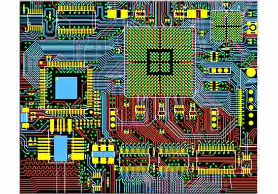
In high-speed design, the continuity of the impedance between the controlled impedance plate and the line is a very important problem. How to ensure the integrity of the signal when the common impedance is 50 euros in one end and 100 euros in difference? In our common way, the adjacent layers of signal lines all have a complete GND plane, or a power plane. We do use single chip microcomputer to do products, generally we do not need to do impedance, it is generally working frequency is very low.
1. Set techniques
Design in different stages need to carry out different Settings, in the layout stage can use large grid points for device layout; For large devices such as IC and non-positioning connectors, the grid accuracy of 50~100mil can be used for layout, while for passive small devices such as resistance capacitors and inductors, the grid accuracy of 25mil can be used for layout. The accuracy of large grid points is beneficial to the alignment and layout of devices. In high-speed wiring, we generally use mm as the unit, we mostly use the unit of mil.
2. PCB layout rules
1. Under normal circumstances, all components are arranged on the same surface of the circuit board as far as possible. Only when the top component is too dense, can some highly limited and small heat devices, such as patch resistance, patch capacitor, patch chip, etc. be placed on the bottom.
2, under the premise of ensuring electrical performance, components should be placed on the grid and parallel to each other or vertical arrangement, in order to neat, beautiful; The element arrangement should be compact, the element in the entire layout should be evenly distributed, the density is consistent.
3, the device as far as possible from the edge of the circuit board is generally not less than 2MM, the process is 5MM from the device, when less than 5MM, we should add the process edge. Of course, the mechanical strength that the board can withstand should also be considered.
3. Layout skills
In the layout design of PCB, the unit of the circuit board should be analyzed, and the layout design should be carried out according to the function. The following principles should be met when the layout of all the components of the circuit is carried out:
1, arrange the position of each functional circuit unit according to the circuit flow, so that the layout is convenient for signal flow, and keep the signal as consistent as possible.
2. Take the core components of each functional unit as the center and carry out the layout around it. The components should be uniformly, integrally and compact arranged on the PCB to minimize and shorten the leads and connections between the components. When the interface is fixed, we should go from the interface to the core component layout. High-speed signal shortest principle.
3. For circuits working at high frequency, distribution parameters between components should be considered. Low frequency and high frequency line circuit to separate, digital and analog circuits to separate design.

4. Layout design
In PCB, special components refer to the key components of the high frequency part, the core components of the circuit, the components susceptible to interference, the components with high pressure, the components with high heat, and some components of the heterosexual element. The positions of these special components need to be carefully analyzed, and the layout of the tape is in line with the requirements of the circuit function and production. Improper placement of them may cause circuit compatibility problems, signal integrity problems, and lead to PCB design failure.
5. Placement order
1. Place components that are closely matched with the structure, such as power sockets, indicators, switches, connectors, etc.
2, place special components, such as large components, heavy components, heating components, transformers, IC, etc.
3. Place small components.
6. Check the layout
1. Whether the size of the circuit board conforms to the processing size required by the CAD drawings.
2. Whether the layout of components is balanced, arranged neatly, and fully distributed.
3. There is no conflict at all levels. For example, whether components, external frames, and connectors are reasonable.
4. Whether the commonly used components are convenient for maintenance and installation. Such as switches, plug-in board insertion equipment, frequently replaced components, etc.
5. Whether the distance between thermal components and heating components is reasonable.
6, whether the heat dissipation is good.
7. Whether the interference of the line needs to be considered.
7. Wiring principles
1. Avoid arranging important signal lines, such as clock and reset signal, at the edge of PCB.
2. The distance between the ground wire of the casing and the signal wire should be at least 2mm
3, high-speed signal as small as possible through the hole, signal to ensure integrity.
4. Whether the number and mode signals are separated. Whether high frequency and low frequency signals are separated.
5. There should be open Windows and heat dissipation holes on the large area copper application design, and the open Windows should be designed into a network.
6, vibration crystal, transformer below the line. These rudiments can only be improved day by day if we practice diligently.
8. Silk-screen display
1, the screen printing position number is not on the solder resistance, after placing the screen printing production is missing.
2, the silk screen position number is clear, the recommended width/height size is 4/25mil, 5/30mil, 6/45mil.
3. Keep the orientation uniform. Generally, do not place more than two directions on a PCB, and the recommended letters are on the left or bottom
9. Check the network DRC and structure
Quality control is an important part of PCB design process. General quality control means include: design self-inspection, design mutual inspection, expert review meeting, special inspection, etc.
Schematic diagram and structural element diagram are the most basic design requirements. Network DRC inspection and structural inspection are to confirm that PCB design meets the two input conditions of schematic diagram netlist and structural element diagram respectively.
10. Regular assembly
In the design, from the perspective of PCB board assembly, the following parameters should be considered:
1. The diameter of the hole shall be determined according to the maximum material condition (MMC) and minimum material condition (LMC). The diameter of the hole for an unsupported component should be chosen by subtracting the MMC of the pin from the MMC of the hole, resulting in a difference between 0.15-0.5mm. And for ribbon pins, the difference in bore diameter between the nominal diagonal of the pin and the unsupported hole will be no more than 0.5mm and no less than 0.15mm.
2. Reasonably place smaller components so that they will not be covered by larger components.
3. The thickness of solder resistance should not be greater than 0.05mm.
4, screen printing identification can not be intersected with any pad.
5. The top half of the circuit board should be the same as the bottom half to achieve structural symmetry. Because asymmetrical boards can become bent.
Shenzhen kingford PCB design capability
Maximum signal design rate: 10Gbps CML differential signal;
Maximum number of PCB design layers: 40;
Minimum line width: 2.4mil;
Minimum line spacing: 2.4mil;
Minimum BGA PIN spacing: 0.4mm;
Minimum mechanical hole diameter: 6mil;
Minimum laser drilling diameter: 4mil;
Maximum number of pins:; 63000 +
Maximum number of components: 3600;
Maximum number of BGA: 48+.
PCB design service process
1. The customer provides schematic diagram to consult PCB design;
2. Evaluate quotation according to schematic diagram and customer design requirements;
3. The customer confirms the quotation, signs the contract and pays the project deposit;
4. Received advance payment and arranged engineer design;
5. After the design is completed, provide the screenshot of the document to the customer for confirmation;
6. The customer confirmed OK, settled the balance, and provided PCB design materials.


Just upload Gerber files, BOM files and design files, and the KINGFORD team will provide a complete quotation within 24h.