
Professional PCB manufacturing and assembly
Building 6, Zone 3, Yuekang Road,Bao'an District, Shenzhen, China
+86-13410863085Mon.-Sat.08:00-20:00

The development of modern science and technology leads to the miniaturization of electronic components and the extensive application of SMT technology and equipment in electronic products. SMT manufacturing units are fully automatic, high precision and high speed. Due to the improvement of automation degree, PCB design has been put forward higher requirements. PCB design must meet the SMT equipment requirements, otherwise it will affect the production efficiency and quality, and may even be unable to complete automatic SMT computer.
SMT and its attributes:
SMT, short for Surface Mounting technology, is an advanced electronic manufacturing technique for soldering and mounting components in specified positions on a PCB. Compared with traditional THT (through-hole technology), the most significant feature of SMT is the increased degree of automated manufacturing, which is suitable for large-scale automated manufacturing.
SMT production line introduction:
The basic integrated SMT line shall contain loader, printer, chip installer, reflow furnace and unloader. The PCB starts at the loader, travels along the path and through the equipment until production is complete. The PCB will then undergo high-temperature welding through the reflow furnace and transfer to the unloader during the printing, installation and welding process.
PCB design elements affecting SMT manufacturing:
PCB design is a key link in SMT technology, and SMT technology is an important factor to determine SMT manufacturing quality. This paper will analyze PCB design elements that affect the quality of SMT equipment from the perspective of manufacturing. The PCB design requirements of SMT manufacturing equipment mainly include: PCB pattern, size, positioning hole, clamping edge, MARK, panel wiring, etc.
1. PCB pattern
In automatic SMT lines, PCB production starts with the loader and is completed after printing, chip installation, and welding. Finally, it will be produced by the unloader as a finished plate. In this process, the PCB is transmitted over the path of the device, which requires that the PCB pattern should be consistent with the path transmission between the devices.
The channel clamping edge is as flat as a line, so this type of PCB is suitable for channel transmission. Sometimes right angles are designed as chamferes.
The path clamping edge is not a straight line, so the PCB position and transmission in the device are affected. Another method is to add a crack edge to the PCB.
2. PCB size
PCB design size must conform to the maximum and minimum size requirements of the SMT machine. So far, most devices are in the 50mmx50mm to 330mmx250mm (or 410mmx360mm) range.
If the PCB thickness is too thin, the design size should not be too large. Otherwise, the reflux temperature will cause PCB deformation. The ideal aspect ratio is 3:2 or 4:3.
If the PCB size is less than the minimum size requirements of the equipment, the board should be assembled. The number of panels depends on the size and thickness of the PCB.
3. PCB positioning hole
SMT positioning methods are classified into two types: positioning holes and edge positions and edge positions. However, the most common method of positioning is Mark point counterpoint.
4. PCB welt pressing
Because the PCB is transmitted along the path of the device, the component must not be placed in the direction of the gripper edge, or the component will be squeezed by the device, affecting the installation of the chip. Some components are placed near the bottom edge of the PCB, so the top and bottom edges cannot be treated as clamping edges. However, there are no components near the two side edges, so the two short edges can be used as clamping edges.
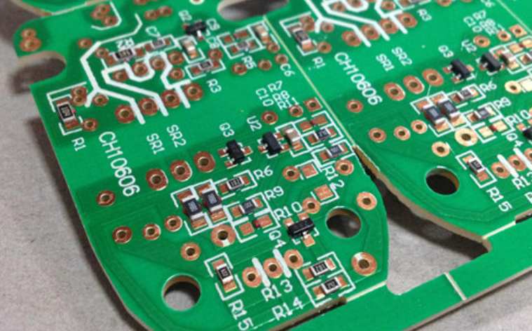
5. Marking
The PCB mark is a point of identification and location for all fully automatic equipment used to correct PCB manufacturing errors.
One. Shape: Solid circle, square, triangle, diamond, cross, hollow circle, oval, etc. Solid circles are preferred.
(1) Size: The size must be within the range of 0.5mm to 3mm. A solid circle with a diameter of 1mm is preferred.
(2) Surface: the surface is the same as the welding plane of PCB welding pad. The welding plane is uniform, neither thick nor thin, and the reflection effect is excellent.
A no-go area shall be placed around the Mark point and other pads, which shall not contain screen printing and solder resistance layers.
6. Splicing method
To improve manufacturing efficiency, multiple small PCBS with the same or different shapes can be grouped together to form panels. For some PCBS with two sides, it is possible to design the top side and the bottom side into one panel, which can produce a template and thus reduce the cost. This approach also helps to reduce top and bottom side shift times, thereby improving manufacturing efficiency and device utilization.
A requirement of the V-groove connection method is to keep the rest of the board (uncut) equal to one quarter to one third of the thickness of the board. If too much circuit board is cut away, the slots may break due to the high temperature of reflow, causing the PCB board to fall off, and the PCB will burn in the reflow furnace.
PCB design is a complex technology that must consider both device requirements and component layout, pad design and circuit design. Excellent PCB design is an important factor in ensuring product quality. This paper presents some issues that should be considered in PCB design from the perspective of SMT manufacturing. As long as we pay enough attention to these problems, automatic SMT manufacturing of SMT equipment can be carried out.


Just upload Gerber files, BOM files and design files, and the KINGFORD team will provide a complete quotation within 24h.