
Professional PCB manufacturing and assembly
Building 6, Zone 3, Yuekang Road,Bao'an District, Shenzhen, China
+86-13410863085Mon.-Sat.08:00-20:00

In PCB design, after the completion of PCB design through many levels, the most important problem is copyright, plagiarism is common. So, how does PCB design prevent others from copying the board? Next, kingford, Shenzhen PCB design company, will introduce you
Common ways to prevent PCB copying board
1, grinding, with fine sandpaper on the chip model to grind off; Works better with a chip with a side door.
2, sealing glue, such as sticking steel, the PCB and its components covered; There are also five or six flying wires twisted together on purpose. It should be noted that the glue can not be corrosive, closed area heating is not too large.
3, the use of special encryption chip, such as ATMEL AT88SC153, etc.
4, the use of uncrackable chips, such as EPLD EPM7128 or above, ACTEL CPLD, etc.
5. Use MASK IC, which requires a large batch.
6, the use of nude, copyists can not see the model and do not know the connection. But it's not too easy to guess what the chip does.
7. Series resistance above 60 ohms on signal lines with small current. (Ha ha, a bit bad, the premise does not affect signal quality).
8. Use some small components without words (or only some code) TO participate in signal processing, such as small patch capacitor, to-XX diode, etc.
9, PCB adopts buried hole and blind hole technology, so that the hole is hidden in the board. (A little expensive)
10, the use of other special accessories, such as customized LCD screen, customized transformer and so on.
11. Apply for a patent. In view of the poor intellectual property protection environment, the best foreign methods in our country can only be put in the last.

2. Introduction to PCBA processing inspection items
In order to avoid production risks in advance, reduce unnecessary process costs, reduce project cycle and improve efficiency, all kinds of complicated design inspection and lengthy evaluation process are essential. Next, the PCBA process inspection item rules are introduced to cover all possible assembly problems, such as:
- Device analysis (distance between components, distance between components and edge, screen printing of components);
- Pin analysis (pin number difference, digit length, patch pin, through pin, press pin);
- Pad analysis (Chip pad spacing/length, pad connection, Mark number), etc.
By checking the rules of PCBA processing items, many kinds of production situations that engineers cannot anticipate in advance can be solved.
1. Spacing between components
Accurately detect pad spacing to avoid mutual interference
2. Device to edge
Accurately detect the distance from the device to the edge of the plate to avoid damaging the device during assembly
3. Screen printing of components
Accurately identify the characters related to the device to avoid mislabeling components due to character digit errors
4. Pin number difference
Check the pin number of pad accurately to avoid the failure of welding of purchased components
5. Bit length
Check the bit number length to avoid SMT machine recognition
6. Patch pin
Accurately detect the area of pad contact pin to avoid affecting welding
7. Through hole pin
Accurately detect the hole size and attribute quantity of through-hole pins to avoid the unavailability of purchased components
8. Press the pin
Accurately detect the hole size and attribute quantity of the press pin, so as to avoid that the purchased components cannot be used
9. Chip pad
Accurately detect the size of Chip pad to avoid bad welding
10. Connect the pad
Accurately identify whether the pad is not wired to avoid open circuit problems
11. Mark counts
Accurately check whether there are mark points in the board and the number of mark points to avoid affecting the patch
12. Marker analysis
Accurately detect the objects around the mark point to determine whether they affect the mark point recognition
kingford is a professional PCB design company engaged in electronic products layout layout design, mainly undertake multi-layer, high density PCB design and circuit board design proofing business. With an average of more than 10 years of work experience in PCB design team, skilled use of market mainstream PCB design software, professional and efficient communication to ensure the progress of PCB design, help you to seize the market opportunity earlier!
PCB design elements affecting SMT manufacturing
Mar 01,2023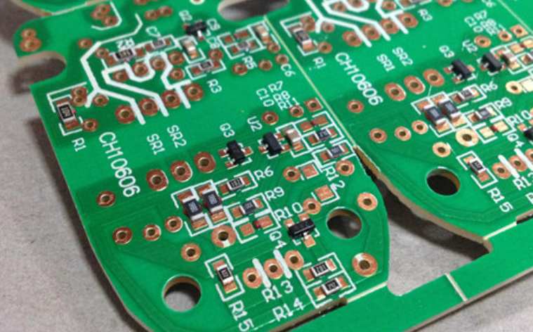


Just upload Gerber files, BOM files and design files, and the KINGFORD team will provide a complete quotation within 24h.