
Professional PCB manufacturing and assembly
Building 6, Zone 3, Yuekang Road,Bao'an District, Shenzhen, China
+86-13410863085Mon.-Sat.08:00-20:00

If the circuit principle of electronic products can be quickly clear, then the efficiency of the work will be twice the result with half the effort. It can greatly improve the efficiency of functional testing and production efficiency of products. So how can we understand the circuit board schematic diagram? To have a deep understanding and understanding of the schematic diagram of the circuit board, it is necessary to have a deep understanding of the circuit, the circuit mainly includes the following several modules of the circuit. The following patch processing manufacturer Xiaobian to explain how to understand the circuit board schematic and PCB design how to route the relevant knowledge.
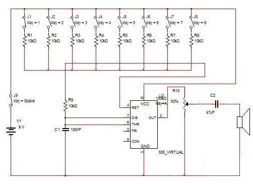
1. How to wire PCB design
PCB design engineers often want to use automatic wiring when designing PCBS. Generally, pure digital circuit board (especially the signal level is relatively low, circuit density is relatively small) using automatic wiring is no problem. However, when designing analog, mixed-signal, or high-speed circuit boards, some problems may arise if PCB design software's automatic wiring tool is used, possibly even serious circuit performance problems. FIG. 1 The top layer of the circuit board designed with automatic wiring FIG. 2 The bottom diagram 3a of the circuit board designed with automatic wiring FIG. 3 The circuit schematic diagram of the wiring in FIG. 1, 2, 4 and 5 FIG. 3b The circuit schematic diagram of the analog part of the wiring in FIG. 1, 2, 4 and 5 For example, Figure 1 shows the top layer of a dual panel with an automatic wiring design. The bottom layer of this dual panel is shown in Figure 2, and the circuit schematics of these wiring layers are shown in Figure 3a and Figure 3b.
Careful consideration was taken to design the mixed-signal circuit board by placing the components manually on the board so that the digital and simulator components could be placed separately. When using this wiring scheme, there are several aspects to pay attention to, but the most troublesome is the grounding. If ground cables are laid on the top layer, the devices on the top layer are grounded through wiring. The device is also grounded at the bottom, and the ground wires at the top and bottom are connected through holes on the far right of the circuit board. When this routing strategy is examined, the first drawback is the existence of multiple ground loops. In addition, it will be found that the ground line return path is cut off by the horizontal signal line. The good thing about this grounding scheme is that the emulator (12-bit A/D converter MCP3202 and 2.5V reference voltage source MCP4125) is placed on the far right side of the board. This layout ensures that no digital ground signals pass under these analog chips. The manual wiring of the circuit shown in Figure 3a and 3b is shown in Figure 4 and Figure 5.
When wiring by hand, to ensure the correct implementation of the circuit, there are some general design guidelines to follow: try to use the ground plane as the current loop; Separate analog ground plane from digital ground plane; If the ground plane is cut off by signal routing, in order to reduce the interference to the ground current loop, the signal routing should be perpendicular to the ground plane; The analog circuit should be placed as close to the edge of the circuit board as possible, and the digital circuit should be placed as close to the power connection as possible, which can reduce the di/dt effect caused by the digital switch. Both dual panels have a ground plane in the bottom layer, which is designed to allow PCBA engineers to solve problems so that they can quickly understand the circuit board routing. Vendor demo boards and evaluation boards often use this routing strategy. However, it is more common to lay the ground plane on top of the board to reduce electromagnetic interference.

2. How do I understand the schematic diagram of the circuit board
In the circuit board industry, whether you are engaged in maintenance work, or functional testing work, if you can quickly clear the circuit principle of electronic products, then the efficiency of the work will be twice the result with half the effort. It can greatly improve the efficiency of functional testing and production efficiency of products. So how can we understand the circuit board schematic diagram? To have a deep understanding and understanding of the schematic diagram of the circuit board, it is necessary to have a deep understanding of the circuit, the circuit mainly includes the following several modules of the circuit. We need to divide the circuit into modules. This is more conducive to our understanding of the circuit board schematic. The main modules of the circuit are:
1, the power circuit: the circuit on the circuit board to work normally, it must provide electricity to the circuit. Therefore, the circuit board must have a power supply circuit.
2, interface circuit: the interface circuit of the PCB circuit board is some input and output interface circuit. For example: connector external circuit.
3, communication circuit: in a sense can be one of the components of the control circuit. Because it has some relatively special circuit communication protocol. Communication circuits can also be called digital circuits. 4, control circuit: control circuit belongs to the digital circuit board. The main function is to control the movement. Including CPLD, CPLD and so on, is an important part of the digital circuit.
5, signal circuit: the main function of the signal circuit is used to control the signal circuit in the circuit, to provide the corresponding signal and signal measurement. Therefore, the signal circuit in general is to simulate the relay circuit.
6, saving circuit: the main function is to store some data in the circuit. Generally divided into serial and parallel saving circuit.

Notes for RF circuit power supply design
Feb 06,2023


Just upload Gerber files, BOM files and design files, and the KINGFORD team will provide a complete quotation within 24h.