
Professional PCB manufacturing and assembly
Building 6, Zone 3, Yuekang Road,Bao'an District, Shenzhen, China
+86-13410863085Mon.-Sat.08:00-20:00


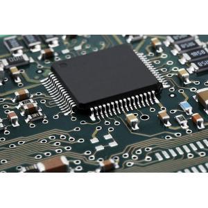
Printed circuit high precision refers to the use of fine line width/spacing, tiny hole, narrow ring width (or no ring width) and buried, blind hole technology to achieve high density. And high precision refers to "thin, small, narrow, thin" results will inevitably bring high precision requirements, take line width as an example: O.20mm line width, according to the regulations to produce O. 16-0.24mm is qualified, its error is (O.20 soil 0.04)mm; And O. 10mm line width, the same error is (0.10 ±O. 02)mm, obviously the latter accuracy increased by 1 times, so it is not difficult to understand, so the high precision requirements are no longer discussed separately. But it is a prominent problem in production technology.
(1) Fine wire technology in the future, high fine wire width/spacing will be 0.20mm-O-13mm-0.08mm-0.005mm, so as to meet the requirements of SMT and Multichip Package (MCP). Therefore, the following techniques are required.
① Thin or ultra-thin copper foil (< 18um) substrate and fine surface treatment technology.
② Using thin dry film and wet film process, thin and good quality dry film can reduce the line width distortion and defects. Wet film can fill small air gaps, increase interface adhesion, improve wire integrity and accuracy.
③ The Electro deposition Photoresist (ED) film was adopted. Its thickness can be controlled in the range of 5-30 / um, which can produce more perfect fine wire, especially for narrow ring width, no ring width and full plate plating. At present, there are more than ten ED production lines in the world.
(4) Using parallel light exposure technology. Because parallel light exposure can overcome the influence of line width variation caused by oblique rays of "point" light source, fine wire with precise line width size and clean edge can be obtained. But parallel exposure equipment is expensive, expensive, and requires a high degree of cleanliness.
⑤ Automatic Optic Inspection (AOI) is adopted. This technology has become a necessary means of detection in fine wire production, and is being rapidly popularized, applied and developed. For example, AT&T has 11 sets of AoI,}tadco has 21 sets of AoI specially used to detect the graphics of the inner layer.
(2) Microporous technology The functional holes of printed boards used for surface mounting mainly play the role of electrical interconnection, which makes the application of microporous technology more important. The use of conventional drill materials and CNC drilling machines to produce small holes has many faults and high costs. Therefore, printed board density is mostly in the wire and pad fineness efforts, although great achievements have been made, but its potential is limited, to further improve the fineness (such as less than O. 08mm wire), the cost rises sharply, so turn to the use of microholes to improve the fineness.
In recent years, the technology of NC drilling machine and micro drill has made a breakthrough, so the micro hole technology has a rapid development. This is the current printed board production of the main outstanding characteristics. In the future, the micro-hole formation technology mainly depends on advanced CNC drilling machine and excellent micro-head, and the small hole formed by laser technology, from the point of view of cost and hole quality is still inferior to the small hole formed by CNC drilling machine.
At present, the technology of CNC drilling machine has made new breakthroughs and progress. And formed a new generation of NC drilling machine which is characterized by drilling tiny holes. The efficiency of micro-hole drilling (less than 0.50mm) is 1 times higher than that of conventional CNC drilling machine, less failure, speed of 11-15r/min; It can drill holes of 0.1-0.2mm, using high quality cobalt drill bit, three plates (1.6mm/piece) can be stacked for drilling. When the bit is broken, it can automatically stop the machine and report the position, automatically change the bit and check the diameter (the tool library can accommodate hundreds of pieces), and automatically control the constant distance between the drilling point and the cover plate and the drilling depth, so it can drill blind holes and won't drill the mesa. CNC drilling machine table using air cushion and maglev, moving faster, lighter, more accurate, will not scratch the table. Such a drill press is very popular at present, such as Italian Prurite Mega 4600, American ExcelIon 2000 series, as well as Switzerland, Germany and other new generation products.
There are many problems with conventional CNC drilling presses and drills to drill tiny holes. It has hindered the progress of micro hole technology, so laser etching has been paid more attention, studied and applied. But there is a fatal disadvantage, that is, the formation of horn holes, and with the increase of plate thickness. In addition to the pollution caused by high temperature ablation (especially for multilayer boards), the life and maintenance of light sources, the repetition accuracy of etching holes and the cost, etc., the popularization and application in the production of tiny holes in printed boards are limited. However, laser etching is still applied in thin and high density microporous plates, especially in McM-l high density interconnection (HDI) technology, such as the combination of mylar etching and metal deposition (sputtering technology) in M.C.Ms. The buried hole formation can also be used in high density interconnected multilayer plates with buried and blind hole structures. However, due to the development and technological breakthrough of NC drill press and micro drill, it has been rapidly popularized and applied. Therefore, laser drilling can not form a dominant position in the application of surface mounted printed boards. But it still has a place in something.

The combination of buried, blind and through hole technology is also an important way to improve the density of printed circuits. Generally, buried and blind holes are small holes, in addition to improving the number of wiring on the board, buried and blind holes are used "recently" interlayer interconnection, greatly reducing the number of through holes, isolation disk Settings will be greatly reduced, thus increasing the number of effective wiring and interlayer interconnection in the board, improve the interconnection density. Therefore, the interconnect density of the buried, blind and through hole combined multilayer board is at least 3 times higher than that of the conventional all-through hole plate structure under the same size and number of layers. If the printed board combined with buried, blind and through hole is under the same technical index, its size will be greatly reduced or the number of layers will be significantly reduced. Therefore, in the high density surface mounted printed board, buried and blind hole technology has been increasingly applied, not only in the large computer, communication equipment and other surface mounted printed board, but also in the civil, industrial field has been widely used, even in some thin plate has also been applied. Such as a variety of PCMCIA, Smard, IC card and other thin six layers of the board.
Buried, blind hole structure of the printed circuit board, generally use the "sub-board" production mode to complete, which means that after several times of pressing plate, drilling, hole plating and so on to complete, so precise positioning is very important.
PCB Introduction to printed circuit boards
Feb 05,2023


Just upload Gerber files, BOM files and design files, and the KINGFORD team will provide a complete quotation within 24h.