
Professional PCB manufacturing and assembly
Building 6, Zone 3, Yuekang Road,Bao'an District, Shenzhen, China
+86-13410863085Mon.-Sat.08:00-20:00

Top level PCB layout recommendations for BGA packaging
As the functions of electronic devices continue to grow, their size is shrinking at the same time. Providing necessary functions for these smaller devices requires the latest development of component packaging technology. Since its introduction in the late 1980s, one of the most popular component packages to meet this demand is the ball grid array (BGA).
Shortly after its launch, BGA packaging became the next big news in packaging technology. They provide higher interconnect density than through-hole PGA and surface mount QFP, and the cost is comparable, without manufacturing problems related to those packages.
Since then, their popularity has continued to rise, and they have become the default package for high pin count integrated circuits, such as microprocessors and storage devices. Let's take a closer look and discuss some PCB layout suggestions for BGA packaging.
Learn more about ball grid array components
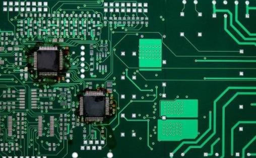
The ball grid array package contains the die of a complex integrated circuit without the pins or leads common to the through-hole or surface mount components. Instead, their needle pads are evenly distributed at the bottom of the package. Each pad in these pads has a tiny solder ball, which is stuck to it by adhesive flux. During reflow soldering of PCB assembly, the solder ball will melt and form a firm joint.
BGA pin pads are determined according to the size and number of device pins, and the spacing is 1.5mm to 0.5mm. The diameter of the welding ball itself ranges from 0.75 mm to 0.3 mm.
With the increase of the number of complex IC pins, the standard surface mount package used before BGA is no longer ideal. These traditionally packaged pins are on the periphery, so the size must be increased to support more pins, which will take up a lot of space on the circuit board. Moreover, with the increase of package size, they began to encounter electrical and manufacturability problems. However, many of these problems have been solved with BGA packaging. Some specific problems have been solved:
Size: BGA pins are evenly distributed under the assembly, rather than depending on the periphery of the assembly leads. This makes the package size of the same number of pins smaller than the parts in the traditional dual in-line package or square flat package.
Performance: Since the pins are distributed at the bottom of BGA, the internal wires connecting the core to the pins are much shorter than those in DIP or QFP packages. These shorter connections reduce their inductance and resistance, thus making the device have better performance.
Thermal resistance: The shorter wires from the tube core to the pin in BGA also reduce the thermal resistance. In this way, the heat generated by the parts can be more evenly distributed to the circuit board, thus helping to cool the parts.
Manufacturing: BGA has much less processing problems than other packages without through hole pins or bent surface mounting leads. BGA solder balls can also be automatically centered during reflow, which helps simplify the manufacturing process.
Reliability: BGA packaging solves the reliability problem of manufacturing high pin number DIP and QFP devices. These packages have the smallest pin width and spacing and can easily form a solder bridge between the pins during assembly.
However, using BGA encapsulation does bring some difficulties. For example, after installing BGA on the circuit board, it is almost impossible to visually inspect the solder joints without X-ray equipment or other advanced scanning tools. However, these problems can be overcome, and the advantages of BGA encapsulation far outweigh their disadvantages.
Next, we will consider some considerations to keep in mind when placing BGA packages during PCB layout.
BGA packaged component placement PCB layout recommendations
The more complex the BGA component you want to use, the more planning you must make to successfully route each pin to its associated network. When the pin spacing of high pin count BGA is 0.5mm, careful planning will be required to design the escape wiring pattern of all its networks. Before you lay out the routing, you need to take a lot of careful consideration on component placement for a long time.
As usual, layout planning starts from fixed components, such as connectors, switches and other IO devices. You also need to keep in mind the heat dissipation considerations of the circuit board to ensure that the hot running BGA has the airflow required to keep cool. The processor and memory chips must be close enough to their off board connectors so that they do not have to walk a long way across the board. At the same time, you must provide enough space for all parts of the signal path so that they are neatly placed, and their routing does not have to go too far to reach them.
When you begin placement, remember to leave enough space for your BGA parts so that they are routed around them. These components should have many associated bypass capacitors and need to be placed directly next to the connected pins. Next, components that are part of the signal path need to be placed sequentially between the source and the load of the signal. This may require changing most of the display location to fit these parts, so be prepared for interactive work to finalize the display location.
Another thing to remember is that in addition to good signal integrity, you need to design for good power integrity. This means that different power supplies are placed near the area they provide, without mixing their circuits with BGA's sensitive digital circuits.
By optimizing the placement of parts, it is time to start routing the BGA network.
Select vias to use in PCB design CAD tools for routing within and around BGA packages.
Connect BGA encapsulated trace route prompt
The first thing to do is to plan the escape wiring or "fanout" from finely spaced surface mounted components (e.g. BGA components). Escape routing is not just drawing a short line and placing a via; It must be planned with component placement, layer stacking, signal integrity requirements, and wiring density. For fine pitch BGAs with high pin counts, additional board layers or high-density interconnect (HDI) cabling strategies may be required. However, before performing this operation, it is always best to contact the PCB manufacturer to confirm the price and its ability to manufacture HDI boards.
When routing the escape cable and via from BGA, start from the outer row. Using diagonal wiring, these traces will be the simplest laying method. From there, you can start working with rows of pins. For BGA with large pin spacing, a short line segment can be used to connect to the through hole beside the pad in the so-called "dog bone pattern".
The large pin spacing BGA will also allow you to route between pads. For smaller spacings, it may be necessary to use through holes on pads, although this will increase the cost of plate manufacturing. Similarly, please contact your manufacturer first to confirm what level of PCB technology they will be able to build for you and at what price. This is the via you will use:
Through hole: This is the most commonly used through hole on the circuit board. They are created with a mechanical drill and run through the board, but the size limit is minimal. For standard width boards, the minimum drilling size is usually not less than 6 mils.
Blind holes and buried holes: These vias can also be created by mechanical drilling, but will only partially penetrate the board, or start and stop at the internal layer of the board. The blind hole can be embedded in the BGA pad. Both the blind hole and the buried hole need to be drilled before the layers of the board are laminated together during PCB manufacturing. These additional steps make the manufacturing cost of blind holes and buried through holes higher, but on compact plates, increasing the cost may be a necessary option.
Micro: These through holes are created by laser and smaller than those drilled by machine, but because of their smaller size, they usually span only two layers. Microwells can be stacked together or staggered side by side to achieve the desired results. Although they are indeed more expensive than mechanical drilling, their ability to seamlessly insert BGA pads makes them very suitable for fanning out of finely spaced parts.
When you wire the escape pattern from the BGA device, remember that components with higher pin counts will require additional circuit board layers. All vias required for wiring from pins will occupy the wiring channel required for routing. You may find yourself having to add another board layer for every two rows of pins on the BGA. The PCB processing factory explained the top PCB layout suggestions of BGA packaging and the latest development of component packaging technology.


Just upload Gerber files, BOM files and design files, and the KINGFORD team will provide a complete quotation within 24h.