
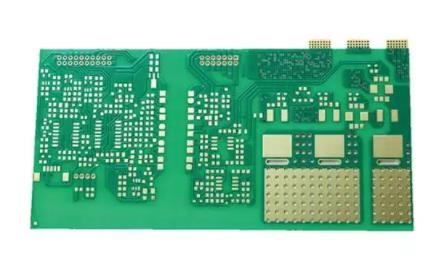
Professional PCB manufacturing and assembly
Building 6, Zone 3, Yuekang Road,Bao'an District, Shenzhen, China
+86-13410863085Mon.-Sat.08:00-20:00

Analyzing more intelligent PCB design can help reduce manufacturing costs
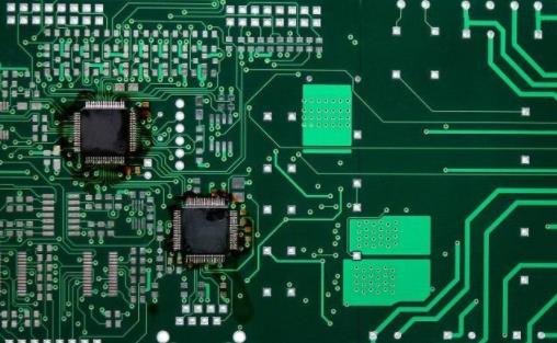
Effective PCB design layout
Careful planning of PCB layout and assembly process is one of the most critical parts in the product development cycle, which requires a lot of due diligence/consideration to avoid expensive performance and/or manufacturing problems.
Suppose you have a great product with excellent circuit performance, but you ignore the assembly considerations. This may lead to low manufacturing yield; The potential high on-site failure rate means that your high-quality products may be priced out of the market soon, and a large amount of product profits will be consumed in rework.
There are many considerations about assembly. We want to think that our contract assembler can handle our products, but small considerations will make a big difference. BOM optimization, limit value, quantity limit of parts on each side, shading and listing are very important, but let's consider the taboo topic for designers: rework design.
Rework design
Should I consider reworking the design? If your goal is to produce a large number of products continuously, especially for products whose profit margins change quarterly, you should do so. This may be due to supply chain fluctuations. Talk with your assembler to understand their rework process and make some considerations in PCB design stage, which can bring huge benefits in the production process. Especially in any RMA process (return authorization), you may have to fulfill your contractual obligations.
Cooperate with your PCB manufacturer
Working closely with PCB manufacturers is a good way to ensure that your design is optimized for your design process, manufacturing process and final assembly. Discuss board stacking, considering long-term production and material availability; Whether there is any supply problem, because if the supplier needs to replace materials in the production process, it is not necessary to re qualify the sensitive circuit.
The design principles communicated and agreed upon in advance allow PCB manufacturers enough time to solve any problems and seek solutions before reaching NPI (new product introduction) and increasing output.
More intelligent PCB design can help reduce manufacturing costs
Design rules and manufacturer's reference design
Many people will think that once the manufacturing stage is reached, it should be smooth sailing. Sadly, the cost will often rise. Failure to follow design rules will lead to a large number of circuit board manufacturing changes and iterations.
Silicon suppliers usually provide reference PCB designs for specific areas of the circuit. Depending on the support they provide, they may require the reference design to be fully replicated. This is not always feasible, because reference designs usually rarely consider mass production and may even be geometrically incompatible with your product. Contact the silicon supplier. Determine the criticality of the circuit area. Try to compromise. Do this as early as possible, as these circuits can often take a long time to qualify.
Design according to IPC standards and combine your own process insights from your own assembler.
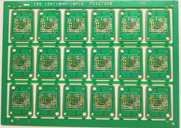
Panel based PCB
Multiple PCBs on a panel enable all these PCBs to be processed simultaneously without having to process them separately. Not only should the circuit boards be made like this, but they should also be assembled and shipped on one panel. There are two aspects to note:
First, you can make better use of standard panels during the PCB manufacturer stage. The more PCBs on a panel, the more cost-effective it is.
Second: During assembly, the more "circuits" on the panel, the better, because the machine can "step and repeat" each circuit. The advantage of this is machine loading and inspection
There is one advantage to producing plates with multiple different plates. You will need to consider final production requirements, potential rework and "x-out" of PCB manufacturer's circuits. You may eventually encounter an inventory imbalance. This may also tighten the part number load that is inserted into the machine. Two parallel lines may be better than one. Evaluate and contact your manufacturer.
Other considerations include rotating the same board to optimize PCB panel space. Therefore, for example, if you have irregular shaped boards, this is a good way to reduce PCB material scrap. The assembly problem you may encounter is the overall increase in insertion time, because the number of rotations performed by the machine is twice that of the original.
It is common to specify the travel direction of PCB panels during assembly. If the same plate is rotated multiple times on one panel, it may lead to inconsistent welding from one product to another. You need to consider these gaps on either side of the device during PCB design. It is established early in the design phase and is easier to implement.


Just upload Gerber files, BOM files and design files, and the KINGFORD team will provide a complete quotation within 24h.