
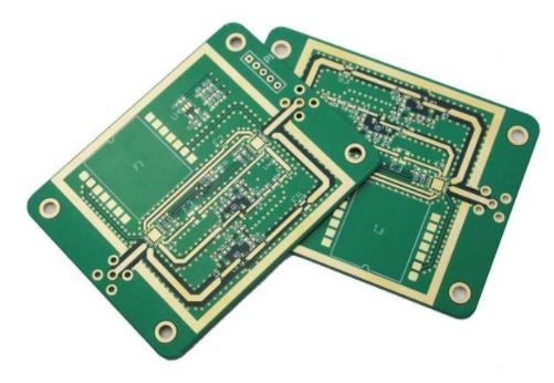
Professional PCB manufacturing and assembly
Building 6, Zone 3, Yuekang Road,Bao'an District, Shenzhen, China
+86-13410863085Mon.-Sat.08:00-20:00

Setting HDI PCB layout and wiring in PCB design software
More advanced PCBs pack more functions in smaller spaces, usually using customized IC/SoC, higher layers and smaller traces. To correctly set the layout of these designs, a set of powerful rule driven design tools is required. These tools can check the routing and layout according to the design rules when creating PCB. If you are using the first HDI layout, it may be difficult to see which design rules need to be set when starting PCB layout.
In this paper, we will study the key design rules to be set when preparing HDI PCB layout, and some techniques to improve efficiency. Altium Designer includes a convenient interface to make these rules easy to access and edit, but the rules shown here are generally applicable to any design platform.
Set HDI PCB layout
For HDI PCB, except for component and wiring density, there is little to distinguish these products from standard PCB. I have seen designers point out that HDI board refers to anything with 10 million or smaller vias, 6 million or smaller wiring or 0.5 mm or smaller pin spacing. Your manufacturer will tell you that HDI PCB uses blind holes of about 8 mils or less, and the smaller blind holes are drilled with laser.
In some aspects, they are correct, because there is no specific threshold for the composition of HDI PCB layout. Everyone can agree that once the design contains micropores, it is HDI plate. In terms of design, you need to set some design rules before touching the layout. Before establishing design rules, you should collect the capabilities of manufacturers. After completing this operation, you need to set up design rules and some layout functions
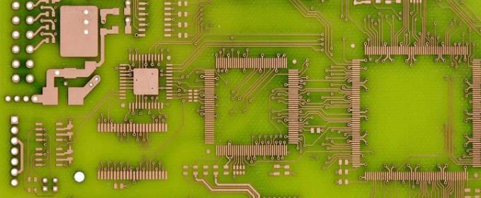
Wiring width and through hole size. The width of a trace with its impedance and routing width will determine when you enter the HDI system. Once the routing width becomes small enough, the through-hole will become so small that it must be fabricated as a micro through-hole.
Layer transitions. The through-hole shall be carefully designed according to the aspect ratio, which also depends on the required layer thickness. Layer transitions should be defined as early as possible so that they can be placed quickly during routing.
Clearance. Traces must be separated from each other and from other objects (pads, components, planes, etc.) that do not belong to the network. The goal here is to ensure compliance with HDI DFM rules and prevent excessive crosstalk.
Other routing restrictions, such as the adjustment of routing length, the maximum routing length and the allowable impedance deviation during routing, are also important, but they will apply to places other than HDI boards. Here, the two most important points are through hole size and routing width. Gaps can be determined in a number of ways (e.g., simulation) or by following standard rules of thumb. Be careful with the latter, as this may lead to excessive inner crosstalk or insufficient wiring density.
Laminations and vias
The HDI stack can range from several layers to dozens of layers to adapt to the required routing density. A circuit board with a high pin count fine pitch BGA can have hundreds of connections per quadrant, so vias need to be set when creating a layer stack for HDI PCB layout.
If you view the layer stack manager in the PCB design software, you may not be able to explicitly define specific layer transformations as micro holes. No problem; You can still set layer transitions and then set through hole size limits in design rules. In Altium Designer, you can create transitions in the Layer Stack Manager and mark them as holes in the Properties panel.
This ability to call microchannels microchannels is useful once you set up design rules and create templates. To set up design rules for routing through vias, you can define design rules to apply only to wells. This allows you to set specific limits for gaps by pad size and hole diameter.
Note that the through-hole width and pad size defined here are derived from the manufacturer's capabilities of earlier projects. Before you start setting up design rules, you should consult the manufacturer about their features. Then, you need to set the routing width in the design rules to ensure that the routing impedance is controlled at the desired value. In other cases, impedance control is not required, and you may still want to limit the wiring width on the HDI board to maintain a high wiring density.
Wiring width
You can determine the required routing width in several ways. First, for impedance controlled routing, you need one of the following tools:
A pen and paper to calculate the required trace size (difficult way)
Online Calculator (Quick Method)
Field solver integrated into your design and layout tools (most accurate method)
This paper discusses the disadvantages of using online calculator to calculate the routing impedance, and the same point of view is also applicable when adjusting the routing size for HDI PCB layout.
To set the route width, you can define it as a constraint in the Design Rule Editor, just as you would with a through hole size. If you are not worried about impedance control, you can set any width. Otherwise, you need to determine the impedance curve of the PCB stack and enter this specific width as the design rule.
As the routing width cannot be too large for the size of via pad, you need to take careful balancing operation. If the routing width of impedance control is too large, the thickness of the laminate should be reduced, because this will force the routing width to decrease, or the size of the pad can be increased. As long as the size of the platform exceeds the value listed in the IPC standard, it is OK from the perspective of reliability.
After determining the width required for impedance control, simply set this value to the design rule. You can use the integrated field solver to define the impedance curve and then use it to enforce the required width in the design rules.
clearance
After completing the two key tasks shown above, you need to determine the appropriate trace gap. Unfortunately, the spacing between traces should not default to the 3W or 3H rule of thumb because these rules are incorrectly applied to advanced boards with high-speed signals. On the contrary, it is better to conduct crosstalk simulation on the proposed routing width and check whether excessive crosstalk will occur. PCB processing factory explanation: HDI PCB layout and wiring are set in PCB design software.


Just upload Gerber files, BOM files and design files, and the KINGFORD team will provide a complete quotation within 24h.