
Professional PCB manufacturing and assembly
Building 6, Zone 3, Yuekang Road,Bao'an District, Shenzhen, China
+86-13410863085Mon.-Sat.08:00-20:00

PCB wiring rules for single ended and differential signals
The distinction between signals that are "slow" or "fast" seems arbitrary and may depend on the person you ask. A related topic is whether PCB routing is "short" or "long" electrically. You may find the same many differences on this topic. Whether you want to route a slow signal or a fast signal in a PCB, you need to follow some PCB routing rules to ensure that your circuit board works as expected.
Before you start routing signals between components, you need to review your design rules and adjust them to meet the signal standards. Before starting to route signals around PCB, you need to set the following important PCB routing rules.
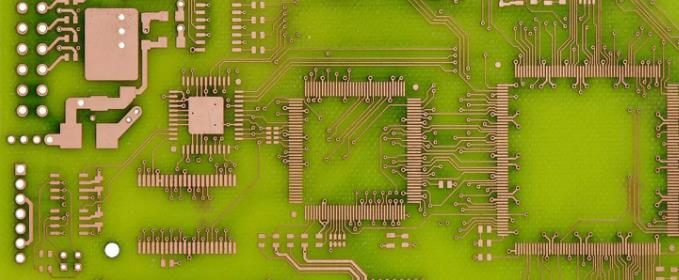
PCB wiring rules for single ended signals
The most important thing to note about PCB routing rules is that the routing standard does not necessarily define itself as "low speed" or "high speed". This difference is created and continued by PCB designers to a large extent, and is largely caused by signal integrity problems when the signal rise time becomes very fast (less than 1 ns). Therefore, when setting design rules, it is particularly important to understand the constraints in the signal standard, whether you are dealing with slow or fast signals.
The first place to find the required design rules is the documentation of signaling standards. Most standard documentation is available online for free. As you create more designs, you will become more familiar with these standards and know what rules are set in the design. Some of the most common PCB wiring rules applicable to many standards for single ended signals are:
Matched length. For bus standard or parallel data routing with source synchronous clock, you need to enforce length matching for all networks in the group within a certain tolerance. When routing, this is accomplished by adding a length adjustment structure to the network.
Through transition. Some standards recommend limiting the number of through-hole transitions to prevent excessive loss, reflection, and other parasitic effects.
Maximum length. Sometimes the maximum length of the net is specified for a given loss tangent value to prevent excessive attenuation of the signal. If you are using a low loss laminate, you can extend the length according to the difference in the tangent value of the loss angle.
Clearance. The trace must be kept separate from other objects (pads, components, planes, etc.) that do not belong to the network. This ensures manufacturability, reduces unnecessary parasitic phenomena, and provides ESD protection in high-voltage designs.
Width and impedance. These two quantities are interrelated and used for the controlled impedance in high-speed design. Learn how to specify impedance and routing width as PCB routing rules.
If you need to assign the same PCB routing rules to a group of networks (very common for single ended signal groups), the fastest way is to assign all the networks in a group to a network category. You can access this function from the Design → Class option (see below) in the PCB Editor window. After assigning nets to categories, you can use the PCB Rules and Constraints Editor to assign design rules to individual nets or network categories.
Other PCB routing rules that may not apply to specific signaling standards are also used to help ensure that your design is in order. Routing topology and routing layer restrictions are two main examples. For more advanced designs, such as components with BGA footprint, you can use design rules to configure fan out policies. Processing differential pairs requires a set of design rules of your own, as shown in the following section.
Differential pair routing rules
Differential pairs are unique because slow and fast signals can be routed as differential pairs. Whether the signal is fast or slow, differential pairs still need to follow some design rules that are usually enforced on single ended signals. Four important design rules to be considered for differential pairs are:
Impedance tolerance. Even if your wiring length is less than the critical length, you'd better bite the sub line to create an impedance curve for the differential pair, unless otherwise specified in your signaling standard. Other geometric constraints will depend on the allowable impedance variation along the differential pair.
Maximum decoupling length. This tells you that the longest distance is that the two sides of the differential pair can remain uncoupled (i.e., a large distance apart). This is important because the uncoupled part looks like an impedance discontinuity, so it must be short enough.
Length matching. Remember that differential signals are read by obtaining the difference between two signals, so the two signals need to arrive at the receiver at the same time. Faster signals require smaller length matching tolerances.
Maximum clear length. Like a single ended signal, a differential signaling standard may have a maximum length limit. Take CAN bus as an example; Even if this is a slow standard, the maximum link length (PCB routing+cable) will depend on the data rate you will use in the system.
You can set design rules for the first two points above in the Routing → Differential Pair Routing area of the PCB Rules and Constraints Editor. The other two points can be solved in the "high speed" area.
If you are using high-speed differential pairs, any other standard high-speed design rules discussed above can be applied to differential pairs. Note that the easiest way is to assign the relevant differential pair to the Differential Pair Network Category, and then select the category that will be controlled by each design rule.
Just like a single ended network, read the documentation on signal standards before you start setting PCB routing rules. Here, you can find the relevant design rule information of the differential signaling standard (usually in the "physical layer" section of the standard). Before you start routing differential pairs, learn how to create impedance curves, assign networks to differential pair network categories, and set some design rules for these categories.
You can assign these PCB routing rules by following the same procedure followed for adding design rules to single ended networks and differential pairs. PCB processing and PCB assembly plants explain PCB wiring rules for single terminal signals and differential signals.


Just upload Gerber files, BOM files and design files, and the KINGFORD team will provide a complete quotation within 24h.