
Professional PCB manufacturing and assembly
Building 6, Zone 3, Yuekang Road,Bao'an District, Shenzhen, China
+86-13410863085Mon.-Sat.08:00-20:00

Introduction to high-speed PCB design: how to eliminate crosstalk
Crosstalk on PCB layouts can have disastrous consequences. If not corrected, crosstalk may cause the finished circuit board to fail to work at all or be troubled by intermittent problems. Let's take a look at what crosstalk is and how to prevent crosstalk in high-speed PCB design.
What is crosstalk in high-speed PCB design?
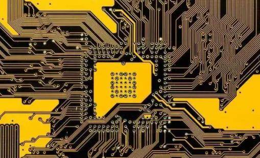
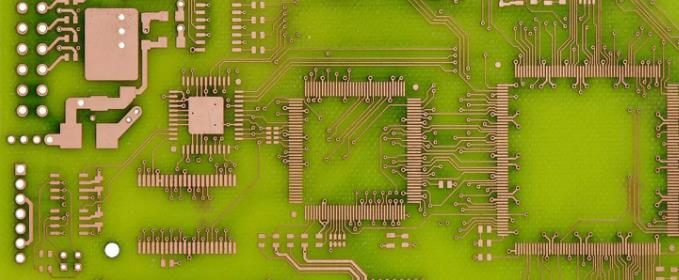
Crosstalk is an unexpected electromagnetic coupling between wires running on a PCB. This coupling may cause the signal pulses of one trace to not work on the signals of the other trace, even if they are not actually in contact with each other. This may occur when the distance between parallel runs is very narrow. Even though traces may maintain minimum spacing for manufacturing purposes, they may not be sufficient for electromagnetic purposes.
Consider that two routes are parallel to each other. If the signal in one trace has a greater amplitude than the other trace, it may seriously affect the other trace. Then, the signal in the "victim" trace will begin to imitate the characteristic impedance of the attacker's trace, instead of transmitting its own signal. When this happens, you will encounter crosstalk.
It is generally believed that crosstalk occurs between two adjacent parallel routes on the same layer. However, crosstalk may occur between two adjacent parallel routes on adjacent layers. This is called wide edge coupling, because the core thickness between two adjacent signal layers is very small, so this is more likely to happen. This thickness can be 4 mils (0.1 mm), sometimes less than the distance between two runs on the same layer.
Eliminate potential crosstalk from high-speed designs
Fortunately, you will not be affected by crosstalk. You can avoid these problems by focusing on high-speed PCB designs that minimize crosstalk. The following are some high-speed design technologies that can help you eliminate the possibility of on-board crosstalk:
The distance between differential pair and other signal routes shall be as large as possible. The rule of thumb is that gap=3 times the trace width.
The difference between clock routing and other signal routing shall be as large as possible. The same gap=3 times the thumb trace width rule is also applicable here.
Keep the distance between different differential pairs as large as possible. The rule of the thumb here is slightly larger, and the gap=5 times the trace width.
Asynchronous signals (such as RESET, INTERRUPT, etc.) shall be far away from bus and high-speed signals. However, since these signals are rarely used in the normal operation of the circuit board, they can be routed next to the on, off, or power on signals.
Ensure that the two signal layers adjacent to each other in the board stack will alternately change the horizontal and vertical wiring directions. By not allowing the routing lines to extend parallel to each other, the chance of wide side coupling will be reduced.
A better way to reduce the potential crosstalk between two adjacent signal layers is to separate the layer between them from the ground plane in a microstrip configuration. The ground plane will not only increase the distance between the two signal layers, but also provide the required return path for the signal layer.
How can design software help you eliminate crosstalk in high-speed PCB design
PCB design tools have many functions built in to help you avoid crosstalk in your design. Circuit board layer rules will help you avoid wide edge coupling by specifying routing directions and creating microstrip stacks. Using network category rules, you will be able to assign larger routing intervals to network groups that are more vulnerable to crosstalk. The differential pair router will route the differential pair together as an actual pair rather than separately. In this way, the required spacing between differential pair routing lines and other networks can be maintained to avoid crosstalk.
In addition to the built-in functions of high-speed PCB design software, there are other tools that can also help you eliminate crosstalk in high-speed PCB design. There are different crosstalk calculators available to help you determine the correct routing width and spacing for cabling. There is also a signal integrity simulator that can analyze whether there is a potential crosstalk problem in your high-speed design.
If crosstalk is allowed, it may be a big problem on the printed circuit board. Now that you know what to look for, you are ready to prevent crosstalk. The design techniques we discuss here and the features in high-speed PCB design software will help you create crosstalk free designs. PCB processing factory explains: What is crosstalk in high-speed PCB design? How to eliminate crosstalk and potential crosstalk?


Just upload Gerber files, BOM files and design files, and the KINGFORD team will provide a complete quotation within 24h.