
Professional PCB manufacturing and assembly
Building 6, Zone 3, Yuekang Road,Bao'an District, Shenzhen, China
+86-13410863085Mon.-Sat.08:00-20:00

Design Skills of Optimal Multilayer PCB for PCB Layout
Designing your first multilayer PCB may not be like the first attempt, but it is still a key step for PCB designers. Next, let's enter the PCB design.
Make sure to set up PCB with multi-layer design
When designing multilayer PCB, you should pay attention to your CAD software first. If you are designing only single or double-sided boards, you may not have set up a multi-layer configuration. Here are three aspects of research:
Negative plane layer: The negative image plane layer is usually used to create power and ground planes on a multilayer PCB layout. Some CAD tools require gaps to be built into pads and overlay shapes in holes drilled in negative plane layers. If you use one of these pcb design software tools, make sure that your pads and package shapes have the correct negative plane gap. If no shape is set for these gaps, a short alignment is created.
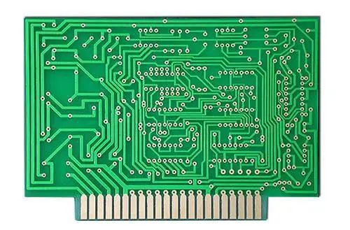
Pad shape on internal signal layer: Some designs use different pad shapes on external layers than on internal layers. For example, the pin 1 pad usually has a square shape for visual identification, rather than a circular shape usually on the inner layer. If your library is not set for a multi-layer pcb configuration, the required pad shape may not be available on the internal signal layer.
Drawing: If you want to create manufacturing and assembly drawings in a layout tool, you may save different logos, tables, and pcb views to the software. For multilayer boards, they must be modified.
Understand the requirements of the processing plant
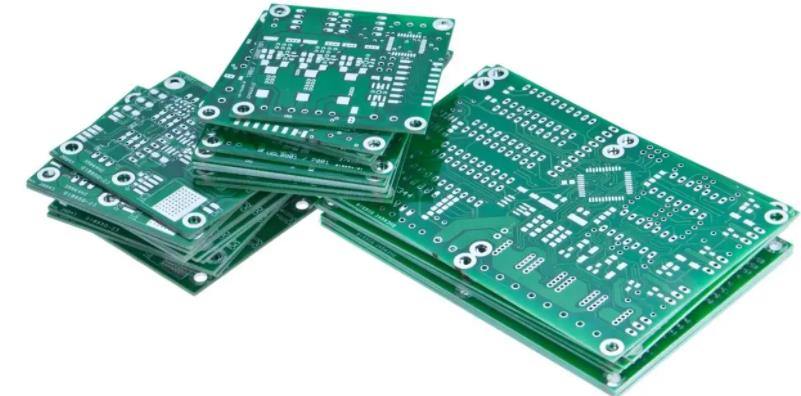
Compared with single-sided and double-sided boards, multi-layer PCB layout design has many important advantages. You can not only save space and increase design density, but also better control signal integrity issues. The key is to work with your manufacturing workshop to understand their requirements for manufacturing multi ply panel designs before you begin.
The processing workshop will have different requirements according to the technical level of the circuit board it can build. Some factories may not be set to build multilayer PCB boards with a specific number of layers or with a very small routing and spacing width. In addition, they may or may not print double-sided PCB layouts. If these limits are exceeded, the manufacturing cost may increase or the circuit board cannot be manufactured as planned.
Take the pass type as an example. Conventional through holes are usually processed in the processing workshop, but they should be checked before using buried, blind or micro holes. As we mentioned, you should also discuss with them the width and spacing of the routing, as well as the number and configuration of slabs. All these factors will affect the manufacturability of PCB, so you should have a clear understanding of them before starting PCB layout design.
Design Skills of Multilayer PCB
Now that your software has been installed and checked in the manufacturing plant, you can design a multi-layer printed circuit board. Here are some useful multi-layer pcb design tips:
The adjacent signal layers are routed in the opposite direction on the printed circuit board. If there are adjacent signal layers on the second and third layers, one shall be wired horizontally and the other vertically. This will help prevent broadband crosstalk problems.
Use the power layer and ground plane. This not only helps distribute power and ground evenly, but also creates microstrip structures that help your signal integrity.
Reduce the size of the internal signal layer through hole pad. Check whether the manufacturing workshop allows smaller inner pads for through hole components and through holes. If so, the reduced pad size will open more wiring channels.
Taking the first step to design a multilayer PCB design can be overwhelming. It may not be as scary as being kicked out of the nest or on a first date, but it may be close! I hope these skills will help reduce your shoulder burden and help you soar in the PCB industry. The PCB processing factory explains the best skills of designing a multilayer PCB and arranging a multilayer PCB.


Just upload Gerber files, BOM files and design files, and the KINGFORD team will provide a complete quotation within 24h.