
Professional PCB manufacturing and assembly
Building 6, Zone 3, Yuekang Road,Bao'an District, Shenzhen, China
+86-13410863085Mon.-Sat.08:00-20:00

Change PCB reference plane during multi-layer circuit board routing
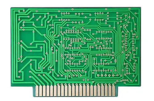
If you are a new designer and have a look at some boards in common electronic products, you may not even realize that they are multilayer boards unless you know exactly where to look. The fact is that more complex devices simply do not allow each trace to be placed on a surface layer, so signals must be routed within the internal layer to make the required connections.
For complex circuit boards involving multiple signals, power supplies and ground planes, your routing strategy is critical to ensure signal integrity and tight coupling with the reference plane. If the correct routing tool is used and the correct strategy is implemented in the design process, there is no need to make difficult repairs to important signal integrity problems.
Routes between layers in the layer stack
To ensure that the multilayer PCB can work as expected, it is necessary to design the correct stack. Lamination will have an important impact on signal integrity, especially EMI in the board and its sensitivity to external radiated EMI. This also determines whether the board can pass EMC inspection after manufacturing.
Your routing strategy and layer stack will need to complement each other. Proper stacking ensures that your routing strategy will eliminate or minimize signal integrity issues. The correct starting point is to consider the grounding plane layout of the signal layer. Each signal layer shall be placed directly near the grounding plane. As long as the routing in the internal signal layer is routed to the components on the surface layer, a ground plane must be placed between the surface signal layer and the internal signal layer. This ensures tight coupling to the PCB reference plane in both layers.
In the above arrangement, if the signal is routed only through a single ground plane, many signal problems can be avoided. When the signal passes through the through hole vertically through the ground plane, it will remain coupled to the ground plane, and its return signal will be sensed in the ground plane. This ensures tight coupling between the entire path and minimizes the loop inductance of the circuit. This also reduces the radiated EMI of the cabling by about 10 dB.
The same idea applies to via wiring across the power plane. Although, it is a good idea to place the power plane near its ground plane. This minimizes the loop inductance, thereby minimizing the susceptibility to EMI and any current induced in the ground plane and power plane. This also increases the capacitance between the planes, providing a low impedance return path for any high-frequency conducted EMI in the power plane.
Reference plane wiring through multiple PCB boards
When wiring through two or more ground planes in a layer stack, the grounding situation becomes more complex. This situation is shown below, where the signal is routed from the inner layer to the surface layer (as shown by the red arrow).
Here, the signal remains tightly coupled with the ground plane in the internal signal layer and the surface layer. However, during the transition from the interior to the surface, there is a region where the signal is not coupled to any region. You can place a via between two ground planes to create a return path during the transition.
If there is no return path, you will suddenly encounter two problems. First, the return path will be formed with the lowest reactance in the nearest grounding element. This is usually a bypass/decoupling capacitor, but it can also be a via connected to the ground plane. When the vias radiate strongly into the transition region, this will cause a large loop inductance in the circuit.
Secondly, a large loop area will increase the sensitivity to external radiated EMI and crosstalk caused by mutual inductance. If there is only one isolated route between two ground planes, as long as low level signals are used, EMI or crosstalk problems need not be worried. If you make multiple of these conversions in a single area, you may need to place multiple vias between planes, or improve stacking and routing strategies.
Don't forget your routing strategy
If you design the correct routing strategy for each signal network before designing the stack, you can eliminate the need to route through multiple planes when switching between surface and internal signal layers. Be careful when using the automatic router; The high-quality auto router will enable you to define specific layer transformations as part of the routing strategy, ideally avoiding the need to route through multiple reference planes.
When designing the BGA fan out strategy, one aspect of the relationship between vertical routing and stacking needs to be considered. For components with a low number of pins, arrange the pins into four lines along the edge of the component (see the figure below). A simple dog bone fan out strategy is sufficient, and only needs to pass through a single ground plane. When using higher pin count packages, you may have no choice but to use two or more ground planes for a single signal network. Make sure to consult the manufacturer's data sheet and maintain the correct grounding to prevent signal integrity problems. Designing multilayer boards and implementing the right strategy ensures that your boards remain signal free. The PCB processing and PCB assembly processing factory explained how to change the PCB reference plane during multi-layer PCB wiring.


Just upload Gerber files, BOM files and design files, and the KINGFORD team will provide a complete quotation within 24h.