
Professional PCB manufacturing and assembly
Building 6, Zone 3, Yuekang Road,Bao'an District, Shenzhen, China
+86-13410863085Mon.-Sat.08:00-20:00

Do you know the basic tools required for PCB design?
Whether you are building a house or a PCB, you need to use the right tools in the toolbox. Every designer needs to have CAD tools for placing parts, but even command line based CAD software can be used to place parts precisely. As modern electronic devices become more and more complex at all levels, designers need tools that help speed up basic design tasks.
Selecting the right PCB design toolset requires weighing many potential options. There are many software packages with different functions on the market, and no one has time to try every software package for free. Some of these design platforms can still be used with outdated workflows that were used 20 years ago. With this in mind, let's take a look at some basic tools that each designer needs to have in their PCB design software.
Schematic design and capture
Your electronic schematic is like the foundation of a house. All the content you put on the board is based on this basic document. This important document shows what components your circuit board needs, how to connect them, and where power and ground are located. With the correct schematic editor, you can easily plan the layout and add notes to the board.
Using the schematic editor can keep your board organized, but once your design becomes more complex, using a single schematic becomes unwieldy. Once you start to include multiple functions on the board, you can keep things organized by using layered schematics. This allows you to divide components into different schematics according to how they are placed in function blocks, and define parent-child relationships between schematics.
Using the multi-channel PCB design tools not only helps you stay organized, but also makes it easy to copy component groups in the hierarchy diagram. Once the schematic is captured as the initial layout, these duplicate component groups are transferred to the new board. You can then begin routing wires between components and placing power and ground connections.
Routing function
Once the schematic is captured as the initial layout, your CAD tools will help you to place components and routing tracks. Cabling is a key task that defines the physical connections between components on the motherboard. For a simple design, it is easy to route each connection manually and check the layout according to the design rules. However, as your circuit boards become more complex and the number of interconnections required increases, tools that automate the routing process can save you a lot of time.
The argument between the advantages of automatic routers and interactive routers seems eternal. For simple circuit boards that do not involve differential pairs, a large number of signal networks or the number of vias on interconnects is limited, the automatic router can still produce a good layout. Note that in these cases, if you can define an appropriate routing policy, the auto router will produce a better layout.
This is where automatic interactive wiring becomes an important PCB design tool. An automatic interactive routing combines the best aspects of automatic routing and interactive routing. You can manually define waypoints for a given signal network along the interconnects. The tool will automatically trace routes in the network between source components, these waypoints and your load components.
Signal integrity and power transmission analysis
In terms of signal integrity, the switching speed of modern digital IC is fast enough to ensure that the signal remains clean, which has become an important consideration for almost all designers. Ensuring signal integrity does require designing the correct stack, routing geometry, and ground plane for your particular application. All of these are tasks of CAD, wiring and circuit board design tools.
If the correct signal integrity software package is used, reflection and crosstalk waveforms in different networks can be checked. This can help you determine when to terminate and which matching network should be used in different traces.
In terms of power transmission and thermal management, by using the power transmission network analyzer (PDNA), you can determine the IR loss in the routing, power and ground planes, and vias. Your PDNA should generate voltage and current density results using an intuitive output format. The best tool will display an interactive color map for you, so that you can visually check the circuit board for potential power cooling problems and excessive IR drop.
PCB design tool based on rule driven engine
Perhaps the most important part of PCB design is to ensure that your design complies with the basic design rules. The design function should check the design data against these rules when creating a layout, so that you can quickly find problems and correct them as needed. Your design rules can also limit the functionality of CAD and routing functions, helping you comply with important design standards.
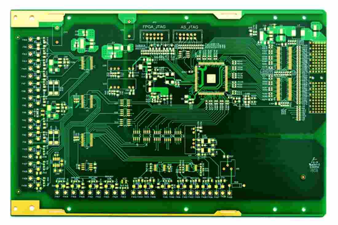
Other PCB design software packages divide these important functions into different programs, forcing you to export and re import data as you move between programs. When a new version is released, you will need to design a complex solution, and there is a real risk that the old data will suddenly become inaccessible. In this environment, workflow and interface are inconsistent among various design tools, which aggravates the learning curve and reduces design productivity. The PCB processing factory explains what tools are needed for PCB design, and what tools each designer needs to master.


Just upload Gerber files, BOM files and design files, and the KINGFORD team will provide a complete quotation within 24h.