
Professional PCB manufacturing and assembly
Building 6, Zone 3, Yuekang Road,Bao'an District, Shenzhen, China
+86-13410863085Mon.-Sat.08:00-20:00

Detailed sharing of digital, analog and grounding in PCB layout
In the field of electronics, I am also confused about the different types of grounding involved in PCB design: digital, analog and grounding. When university lecturers always point out that although the reasons have the same reference, they are expressed in different symbols, it is difficult not to be confused.
Theoretically, it is easy to understand that digital electronic components refer to digital ground, and so do analog electronic components. They can be clearly distinguished by the grounding symbol used in the schematic diagram. However, the real challenge is to physically wire and place the respective grounding on the PCB.
What is the ground actually doing?
Digital current, whether single point grounding current or appropriate grounding scheme with reference point, grounding pin and grounding tester, is used for measurement of digital circuit. Whether you want to combine anti aliasing filters or differential amplifiers, analog-to-digital converters and other components, or be alert to the signal and noise differences in equipment or power supplies with signal-to-noise ratio and voltage, you need to know what you are looking for.
Sometimes, you need to re understand the basics to master the grounding technology in PCB design. This means going beyond the schematic symbols on the ground. In a typical electronic system, the ground provides a reference for digital and analog signals. Therefore, in order to obtain reliable signals, the ground must be relatively "clean".
The ground also acts as a return path for the current flowing through the signal wiring. There are two things to remember about the current path:
The current always flows through the path with the least resistance.
The grounding wire must be large enough to handle any large current.
Digital, analog and grounded
Digital circuits are usually characterized by a rapid transition of signals oscillating between Vcc and 0V. Naturally, the ground will suffer spikes when current pulses pass through. On the other hand, analog signals rely heavily on stable grounding to provide accurate readings.
Grounding actually refers to the physical connection extending to the earth itself. It is usually connected to the chassis or used to safely transmit electrostatic discharge from adjacent components. Theoretically, the earth is a neutral electric plane. However, it turns out that sometimes it can be noisy.
Connect different grounds on the PCB
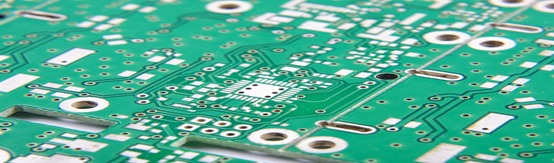
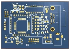
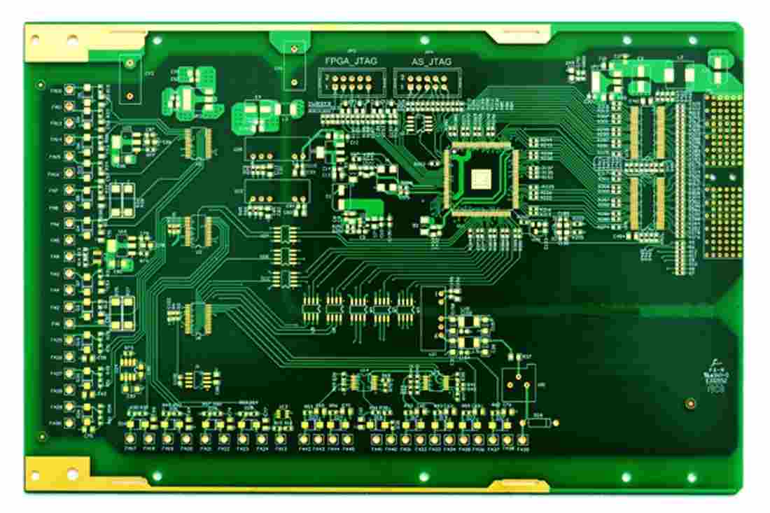
Even for experienced engineers, correctly setting the grounding pattern on the PCB is a thorny problem. For example, an error in audio and digital grounding can cause static noise to couple to the audio output. New designers can only use a single ground plane, resulting in random fluctuations in analog inputs. The PCB processing factory explains the detailed sharing of digital, analog and grounding in PCB layout, and different types of grounding involved in PCB design.
Some electronics experts point out that star connection is one of the best ways to connect various types of grounding at a single point. However, in some cases, star connection may not be feasible due to component layout or space limitations on the PCB.
After making many mistakes in grounding connection, I finally learned how to design a stable grounding. I prefer to use the grounding bar method and isolate the power supply, digital and analog modules on the PCB board.
Of course, this grounding method is only applicable when the components can be clearly separated according to their functions. The principle of ground plane arrangement is to place the noisiest grounding terminal at one end and the most sensitive grounding terminal at the other end.
In some cases, it is only necessary to separate the ground plane at a specific component. This can be done by separating the ground plane below the component in the following ways:
Grounding on PCB boards should not be considered a proprietary topic. Instead, pcb designers should use common sense, or rather, the basic laws of electronics and vivid imagination, to visualize how electrons travel along the path formed by different grounding arrangements.


Just upload Gerber files, BOM files and design files, and the KINGFORD team will provide a complete quotation within 24h.