
Professional PCB manufacturing and assembly
Building 6, Zone 3, Yuekang Road,Bao'an District, Shenzhen, China
+86-13410863085Mon.-Sat.08:00-20:00

Drawing requirements for flexible PCB in PCB design
In order to successfully design flexible PCB, it is important for designers to have a basic understanding of flexible drawing requirements.
Let's take a closer look at these eight drawing requirements:
Flexible PCB stack construction and layer sequence
Dimensional drawings and tolerances
Flexible PCB materials used
Specifications
Borehole symbol diagram
Flexibility (bending radius)
Plating requirements
Test requirements
Marking requirements
1. Flex PCB stack structure and layer sequence:
A PCB stack distinguishes between a rigid layer and a flexible layer in a PCB. The flexible PCB stack will give the thickness of each layer, including the copper thickness of the conductive layer. This should also show which layers are rigid and which layers are flexible including copper weights.
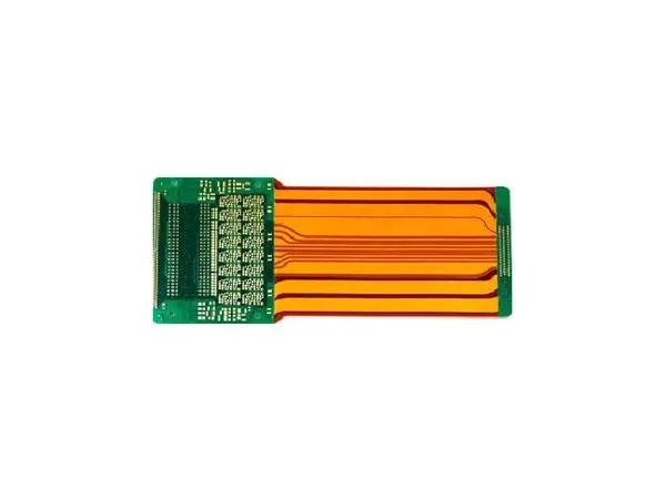
Sample 4-layer flexible PCB stack
2. Dimensional drawings and tolerances
Dimension icons identify many key measurements for PCB design. It should define a rigid to flexible interface (where the two types of materials meet). The typical profile tolerance is+/- 0.010 inch.
The dimension drawing of flexible PCB design provides the following information:
Position and size of PCB stiffeners
Thickness and materials of PCB parts
Type of static or dynamic flexibility during circuit operation. A PCB bent up to 20 times is called a semi static flexible PCB. A PCB that is bent and twisted periodically is called a dynamically bent PCB. The printer uses a dynamic flexible PCB because the circuit bends during the entire operation of the printer.
The position where the circuit board is rarely bent and often bent.
3. Flexible PCB materials used
It is very important to select the correct PCB material for your flexible PCB design, because it will affect the overall performance of the flexible PCB. Before starting the selection, we need to ensure that the material properties meet your specific board requirements and final application. It is important to mention which type of material will be used in your flexible PCB manufacturing process. Flexible PCB materials include:
Flexible dielectric materials
Conductor (copper type)
PCB stiffener
4. Specifications
PCB manufacturers expect a wide range of specific details
PCB manufacturers expect designers to provide the following specific scope details.
Class type (Class 1, Class 2, Class 3), wiring type and installation requirements
Flexible copper clad materials used
Coating material
Maximum plate thickness
Minimum size of plated through hole
Electrical test requirements
Cover color
Silk screen color
Board markings, such as part number, version, and company logo
Packaging and transportation requirements
Minimum conductor width and spacing
Special packaging requirements (if any)
5. List of drilling symbols
The drilling symbol table indicates all finished hole sizes and hole size tolerances for the board design. To learn more about PCB drilling, read PCB Drilling Instructions: What to Do and Don't Do. The drilling symbol table summarizes the drilling information that exists on the plate. An example of a drill through symbol chart is shown below. The standard finished hole size is+/- 0.003 inch, but it has never been assumed, so this size must be indicated on the design drawing.
PCB drilling symbol table.
Each symbol represents the bit size. The other columns in the chart provide information like the shape of the hole, and the type of hole (through or without plating).
6. Flexibility (bending radius)
The flexibility of flexible PCB depends on the bending radius of the flexible material used. The bending radius is the minimum angle at which the bendable area can be bent. The figure below helps us understand the concept of bending radius.
It is important to specify the bending radius of the flexible PCB
Knowing how many times a flexible PCB bends is critical to your design. If the PCB is bent more than the design allows, the copper will begin to stretch and crack.
The bending radius depends on the number of layers and the type of material used in flexibility.
To learn more about flexible design considerations, please read our article to avoid common flexible PCB errors and successful designs.
7. Plating requirements
Multilayer PCB requires plating through hole or through hole. It is important to mention the type of plating required for your flexible PCB. The available plating types are:
Panel electroplating
Pattern electroplating
Pad electroplating
Panel Plating: This plating method will deposit copper on the entire panel. This type of plating is usually performed before the circuit is imaged.
Pattern plating: This type of plating deposits copper on the selected area of the flexible PCB.
Only pad plating: This is a pattern plating. Image resist covers the entire panel, while pads capture vias. As a result, only through holes and bare pads are plated.
In the Sierra circuit, we use the selective plating process "only the backing plate" to plate copper in the through-hole. In order to do this, we drill holes in the flexible copper clad dielectric material, and then image the "pad board" image around the drill hole at a resolution of (drill hole diameter) D+0.003 "or higher. In use approx After the 001 inch copper electroplating hole, we again used the completed circuit pattern to image and etch the required pattern. This etching process requires an additional D+0.014 inch pad, which makes our minimum pad size on double-sided flexible products reach the drilling diameter+ 017。” These pads should always be the same size as the design allows.
8. Test requirements
Physical and electrical testing requirements (type and frequency of testing) shall be mentioned. When specifying tests, the designer should consider the requirements very carefully. Overspecifying test requirements may increase overall circuit costs. PCB testing includes:
Dimension inspection
Electrical continuity
inductance
capacitance
Ion cleanliness
flexibility
Plating thickness
insulation resistance
9. Marking requirements
The manufacturer wants the designer to specify the type of ink used for various plate markings, such as serial numbers, component mounting locations, stiffener/cover locations, and panel based markings. Ink types include:
Durable white ink
Traditional epoxy ink fingerprint
When we design flexible PCBs, it is crucial for us to provide important information (drawing requirements) to manufacturers, because this information helps them to manufacture flexible PCBs according to designers' expectations without any time delay. It is important for PCB assembly and PCB processing manufacturers to explain that flexible PCB has a basic understanding of flexible drawing requirements.


Just upload Gerber files, BOM files and design files, and the KINGFORD team will provide a complete quotation within 24h.