
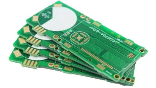
Professional PCB manufacturing and assembly
Building 6, Zone 3, Yuekang Road,Bao'an District, Shenzhen, China
+86-13410863085Mon.-Sat.08:00-20:00

What are the main processes and precautions of PCB design?
How much do you know about PCB? According to the number of layers of PCB, it can be divided into single panel, double panel, four layer board, six layer board and other multi-layer boards. The advantages of PCB greatly reduce the errors in wiring and assembly, improve the level of automation and production, and constantly develop towards high-precision, high-density and high reliability. Next, let me introduce to you the main process of PCB design? What should be paid attention to in PCB design?
1、 What is the main process of PCB design?
1. System specifications
First of all, plan out the system specifications of the electronic equipment. It includes system functions, cost limits, size, operation conditions, etc.
2. Functional block
(1) Next, we must make a functional block diagram of the system. The relationship between squares must also be marked.
(2) If the system is divided into several PCBs and the system is divided into several PCBs, it can not only reduce the size, but also enable the system to upgrade and exchange parts. The system function block diagram provides the basis for our segmentation. For example, a computer can be divided into a motherboard, a display card, a sound card, a floppy disk drive, a power supply, and so on.
(3) Decide to use the packaging method and the size of each PCB When the technology and the number of circuits used by each PCB are determined, the next step is to decide the size of the board. If the PCB design is too large, the packaging technology will be changed or the segmentation will be performed again. When selecting technologies, the quality and speed of the circuit diagram should also be taken into account.
2、 What should be paid attention to in PCB design?
1. Avoid arranging important signal lines at the edge of PCB, such as clock and reset signal.
2. The space between the casing ground wire and the signal wire shall be at least 4mm; Keep the length width ratio of enclosure ground wire less than 5:1 to reduce inductance effect.
3. The devices and wires with confirmed positions shall be locked with the LOCK function to prevent them from misoperation in the future.
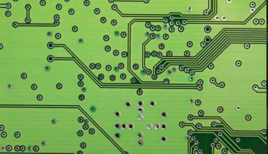
4. The minimum width of the conductor shall not be less than 0.2mm (8mil). In high-density and high-precision printed circuit, the width and spacing of the conductor can generally be 12ml.
5. The principles of 10 - 10 and 12 - 12 can be applied to the wiring between the IC pins of DIP package, that is, when two pins pass through two wires, the pad diameter can be set to 50 mil, and the line width and line spacing can both be set to 10 mil. When only one wire passes between two pins, the pad diameter can be set to 64 mil, and the line width and line spacing can both be set to 12 mil.
6. When the diameter of the pad is 1.5mm, in order to increase the peeling strength of the pad, round pads with a length of no less than 1.5mm and a width of 1.5mm can be used.
7. When the wiring of pad connection is thin, the connection between pad and wiring shall be designed as a water drop, so that the pad is not easy to peel and the wiring is not easy to disconnect from the pad.
8. In the design of large-area copper coating, there shall be a window on the copper coating, with heat dissipation holes, and the window shall be designed as a mesh.
9. Shorten the connection between high-frequency components as much as possible to reduce their distribution parameters and mutual electromagnetic interference. Components susceptible to interference shall not be too close to each other, and input and output components shall be as far away as possible.
The above is my opinion on "What is the main process of PCB design? What should I pay attention to in PCB design?" The introduction of, provide for everyone to refer to, wish everyone a happy life!


Just upload Gerber files, BOM files and design files, and the KINGFORD team will provide a complete quotation within 24h.