
Professional PCB manufacturing and assembly
Building 6, Zone 3, Yuekang Road,Bao'an District, Shenzhen, China
+86-13410863085Mon.-Sat.08:00-20:00

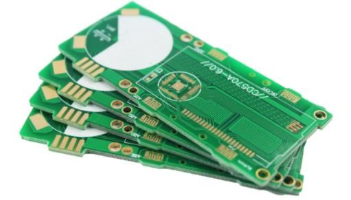
Detailed explanation of high-speed PCB image layer design
In high-speed multilayer PCB, the mirror layer plays an important role in noise control. A good design of the mirror layer can reduce the noise caused by stray inductance and help to control crosstalk, reflection and electromagnetic interference. This paper focuses on the application of local ground plane in combination with the author's actual design, and gives an example of a digital analog mixed circuit to show a method of image layer segmentation and some problems needing attention in practice.
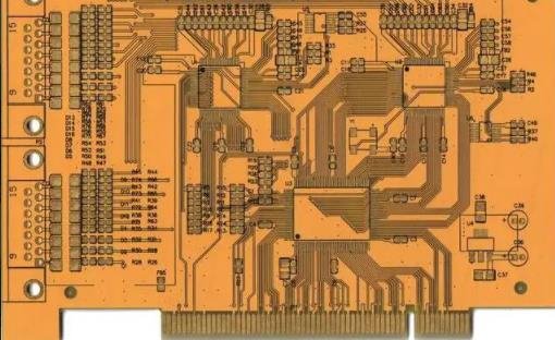
Nowadays, most high-speed circuit systems use multilayer boards, and many circuit systems have multiple working power supplies, which puts forward strict requirements on the design of the mirror layer, especially how to handle the relationship between multiple power (ground) layers. In addition, some systems also need to design special copper coating planes in the device layer to suppress RF energy generated by the oscillator and provide good heat dissipation for high-power power devices.
1、 The role of the mirror layer
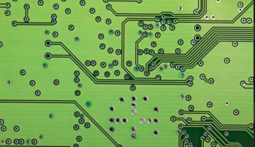
The mirror layer is a layer of copper coating plane (power layer, ground plane) adjacent to the signal layer inside the PCB, which mainly has the following functions:
Reduce return noise and electromagnetic interference (EMI). The mirror layer can provide a low impedance path for signal return, especially when there is a large current flow in the power distribution system
Display. In addition, the existence of the mirror layer reduces the area of the closed loop formed by the signal and return flow, and reduces EMI.
It is helpful to control the crosstalk between signal lines in high-speed digital circuits. The crosstalk is determined by the ratio D/H. D is the distance between the interference source and the disturbed object, and H is the height of the signal line from the mirror layer. By changing H, the ratio D/H can be controlled to control the crosstalk between signal lines.
It is beneficial to impedance control. The characteristic impedance of the printed wire is related to the width of the wire and the height of the wire from the mirror layer. If there is no mirror layer, we may not be able to control the impedance, so that we cannot match the transmission line, resulting in the reflection of the signal.
In addition, the mirror layer can also control the noise radiated to the outside of the board. Of course, the optical mirror layer is not enough to play these roles, and must be supplemented by strict design rules to achieve the desired goals. It can be described as follows: in high-speed digital circuits, it is necessary to control the noise image layer, but it is not enough to have an optical image layer.
2、 Inter layer jump of signal return
In a multilayer PCB, each wiring layer should be adjacent to a mirror layer, and the return current of the signal flows on its corresponding mirror layer. When the signal line from the source to the load cannot be routed in one wiring layer, the usual approach is to connect the signal line to one wiring layer (such as the x-axis), and then use the through-hole to connect the signal line to another layer (such as the Y-axis). Then, when the signal line jumps from one layer to another, the return current should also jump from one layer to another with the line. If both layers are layers, the return current can jump through the through hole connecting the two layers or the grounding pin of the device.
If one is the power layer and the other is the layer, the only opportunity for the return current to jump between the two layers is to place the decoupling capacitor. If there is no decoupling capacitor or through hole connecting to the formation near the jump point, the return current must be wound to a far place to realize jump. As a result, the return current is coupled to other circuits, causing crosstalk and electromagnetic interference problems.
Therefore, in PCB design, the interlayer jump should be carried out near the grounding pin or decoupling capacitor of the adjacent device as far as possible. If this is not possible, the jump of the return current can be realized by placing a ground through hole (the return current jumps between two ground layers) or a bypass capacitor (the power supply layer jumps between the ground layers) near the jump point. The circuit board manufacturer will explain a method of image layer segmentation and some problems that need attention in practice.


Just upload Gerber files, BOM files and design files, and the KINGFORD team will provide a complete quotation within 24h.