
Professional PCB manufacturing and assembly
Building 6, Zone 3, Yuekang Road,Bao'an District, Shenzhen, China
+86-13410863085Mon.-Sat.08:00-20:00

Some Experiences on Line Width and Copper Laying through Holes in PCB Design
First, I'll tell you a little bit of wiring knowledge (it's all my hard work, not forwarding), and then I'll talk about the actual situation. Please be patient.
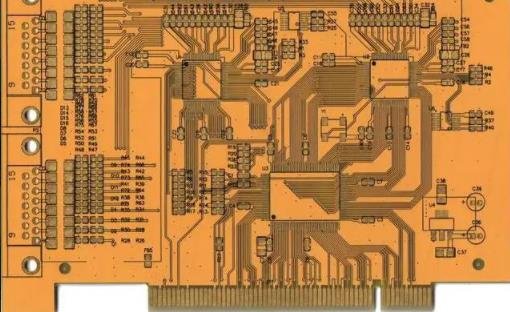
We generally have a common sense when drawing PCB, that is, thick lines (such as 50mil or above) can be used in places with high current, and thin lines (such as 10mil) can be used for signals with low current. For some electromechanical control systems, sometimes the instantaneous current flowing through the wiring can reach more than 100A. In this case, the thin wire will definitely have problems. A basic empirical value is: 10A/mm2, that is, the current value that can safely pass through the wiring with a cross-sectional area of 1 mm2 is 10A. If the wire width is too thin, the wire will be burnt when the large current passes through. Of course, the energy formula should also be followed when the current is burnt out: Q=I * I * t. For example, for a 10 A line, a 100 A current burr suddenly appears, and the duration is US level. Then the 30 mil wire can certainly withstand. (Another problem arises at this time? Stray inductance of the wire. This burr will generate a strong reverse electromotive force under the effect of this inductance, which may damage other devices. The thinner and longer the wire is, the larger the stray inductance is. Therefore, the length of the wire should be considered in practice.)
General PCB drawing software often has several options for copper coating of via pads of device pins: right angle spokes, 45 degree angle spokes, and straight laying. What's the difference between them? The novice usually doesn't care much about it. Just choose one at random. It's beautiful. Actually not. There are two main considerations: first, it is necessary to consider not to dissipate heat too fast, and second, it is necessary to consider the over-current capability.
The feature of using direct laying is that the pad has a strong over-current capacity. This method must be used for device pins on high-power circuits. At the same time, its thermal conductivity is also very strong. Although its operation is beneficial to the heat dissipation of devices, it is a problem for circuit board solders, because the pad heats up too quickly and it is not easy to hang tin. It often requires a larger wattage soldering iron and a higher welding temperature, reducing the production efficiency. The use of right angle spokes and 45 angle spokes will reduce the contact area between the pin and the copper foil, so the heat dissipation is slow, and the welding is easier. Therefore, the connection mode of copper laying for via pads should be selected according to the application situation, and the over-current capability and heat dissipation capability should be considered together. The low-power signal wire should not be directly laid, but the pads passing through the high current should be directly laid. As for right angle or 45 degree angle, it looks beautiful.
Why did you mention this? Because I have been studying a motor driver for a while, the H-bridge device in this driver is always burnt out, and I can't find the reason for it for four or five years. After a lot of hard work, I finally found that the bonding pad of a device in the power circuit used the right angle spokes to pave copper (and only two spokes actually appeared due to poor copper painting). This makes the overcurrent capability of the whole power circuit greatly reduced. Although the product has no problems during normal use, it works normally under 10A current. However, when the H-bridge is short circuited, a current of about 100A will appear on the circuit, and the two spokes will be burnt out instantaneously (uS level). Then, the power circuit turns into an open circuit, and the energy stored on the motor is emitted through all possible ways without a drain channel. This energy will burn the current measuring resistor and related operational amplifier devices, destroy the bridge control chip, and enter the signal and power supply of the digital circuit, causing serious damage to the entire equipment. The whole process is as thrilling as detonating a large mine with a hair. Then you may ask why only two spokes are used on the pad in the power circuit? Why don't you let the copper foil go straight? Because, hehe, people in the production department said that the pin was too difficult to solder! The designers listened to the production staff, so they did PCB processing and PCBA processing manufacturers will explain to you their experience in PCB design on line width and via copper laying.


Just upload Gerber files, BOM files and design files, and the KINGFORD team will provide a complete quotation within 24h.