
Professional PCB manufacturing and assembly
Building 6, Zone 3, Yuekang Road,Bao'an District, Shenzhen, China
+86-13410863085Mon.-Sat.08:00-20:00

Introduction to PCB Design Layout Guide for Engineers
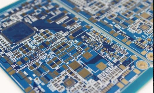
Printed circuit board layout goes far beyond its appearance. A successful PCB layout will make its circuits physically arranged to achieve better electronic performance of the circuit board, and at the same time, it can be completely manufactured. This requires careful management of library components, CAD settings and parameters, component placement, routing, and design of the power supply network (PDN). In addition, layout designers must ensure that their work is fully documented and that the final product is ready to be included in the main electronic systems they design.
This is a lot of work to do, especially for engineers who are not familiar with the PCB layout process. To help complete this workflow, it is recommended to have a comprehensive set of circuit board layout guidelines for reference. Industry and enterprise standards will specify the details of the design, but layout guidelines are important to help engineers navigate the board development process from start to finish. The following are some basic PCB design layout guidelines that can be used to develop your own PCB development guidelines.
Before Layout Start
Before the layout process starts, several tasks need to be handled to ensure the success of the design, first of all, the PCB packaging library to be used.
When building libraries for your PCB layout, it is important to use industry standards (such as IPC) or manufacturer specifications for package sizes and dimensions. However, individual, company or technology needs may also determine changes in some parts. For example, packages in RF designs may require smaller pad sizes than standard digital designs. Here are some additional guidelines for building your own PCB assembly package:
Make sure that any library assembly you build has an acceptable pad pattern size and its spacing meets the standard for that assembly.
PCB packaging needs to include all necessary elements, such as part outline, silk screen mark and reference mark.
A good rule of thumb is to ensure that your manufacturer can build the parts you are designing before submitting them to the final design.
Another option is to use PCB packaging from an external CAD library vendor. Parts manufacturers usually pre build their own components for your design system, and some tools have browsers to easily download these parts.
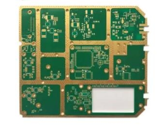
Board profile and layer stacking
Before you begin the board layout, you need to work with the mechanical designer to get a good outline shape. Although the shape factor of the design can be changed in the future, any change may force a large number of redesigns of the circuit to adapt to the new shape. In addition, most CAD tools will accept data imported from mechanical design systems, making your work easier. However, even if you use imported data, you still need to ensure that the board outline is correct and contains all the necessary CAD elements for your design, such as forbidden areas.
Layering shall also be completed prior to the start of the layout. Again, these can be changed later, but the potential impact on existing circuits can disrupt your design schedule and budget. The layer stack should also be fine tuned for your specific design to ensure the correct layer configuration for impedance control routing and other signal integrity requirements. It is also important to select the circuit board material at this stage, so that the appropriate routing width and other design calculations can be carried out according to the physical characteristics of the material. These characteristics include dielectric constant, insulation quality, moisture absorption and dissipation coefficient.
CAD parameters and settings
It is not uncommon to find designers working with the default settings that come with their CAD systems. However, most CAD systems provide users with wide fan control over color, hatch pattern, shadow, font size and width. You can also change the display of certain objects, place one design element on top of another, set the grid, and specify layout and routing preferences. These settings are designed to improve your productivity, and you can save time by spending time optimizing settings in advance. Explanation of circuit board assembly and circuit board processing manufacturers: a guide to the design and layout of circuit boards for engineers.


Just upload Gerber files, BOM files and design files, and the KINGFORD team will provide a complete quotation within 24h.