
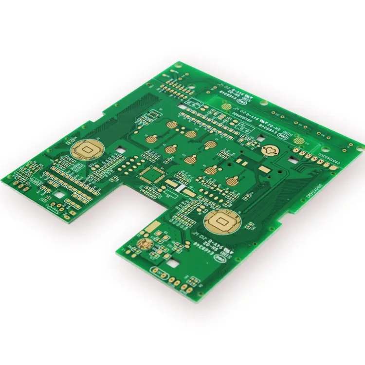
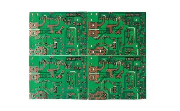
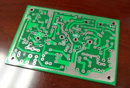
Professional PCB manufacturing and assembly
Building 6, Zone 3, Yuekang Road,Bao'an District, Shenzhen, China
+86-13410863085Mon.-Sat.08:00-20:00

Explain and share the skills of writing PCB design rule checker
This paper describes a method of writing PCB design rule checker (DRC) system. After PCB design is obtained by using the circuit diagram generation tool, DRC can be run to find any fault that violates the design rules. These operations must be completed before the subsequent processing starts, and the developer of the circuit diagram generation tool must provide the DRC tool that most designers can easily master.
Writing your own PCB design rule checker has many advantages. Although the design checker is not so simple, it is not unattainable, because any designer familiar with existing programming or scripting languages can completely design the checker. The benefits of this work are incalculable.
However, general tools for marketing are often not flexible enough to meet specific design needs. Therefore, customers must reflect new feature requirements to DRC tool developers, which usually requires a certain amount of money and time, especially when the requirements are constantly updated. Fortunately, most tool developers can provide customers with convenient ways to write their own DRCs to meet specific needs. However, this powerful tool has not been widely recognized or used. This article provides a practical guide to maximizing the benefits of DRC tools.
Because DRC must traverse the entire PCB design circuit diagram, including each symbol, each pin, each network, and each attribute, it can also create unlimited "attached" files if necessary. As described in Section 4.0, the DRC may indicate any minor deviations from the design rules. For example, one of the attached documents may contain all decoupling capacitors used in the design. If the capacitance is lower than or higher than the expected value, a red mark [1] will be marked where the dv/dt problem of the power line may occur. These attached files may be necessary, but not all commercial DRC tools can create these files.
Another advantage of DRC is that it is easy to update to meet the needs of new design features (such as those that may affect the design rules). Moreover, once you have gained sufficient experience in this field, you can realize many other functions.
For example, if you can write your own DRC, you can write your own BOM creation tool, so that you can better handle specific user needs, such as how to obtain "additional hardware" (such as sockets, heat dissipation devices or screwdrivers) for devices that are not part of the circuit diagram database. Or designers can write their own Verilog netlist analyzer, which has sufficient flexibility in the design environment, such as how to obtain Verilog models or time files applicable to specific devices. In fact, since DRC traverses the entire design circuit diagram, all effective information can be collected to output the simulation and/or BOM required for PCB design Verilog netlist analysis.
It is far fetched to discuss these topics without providing any program code. For this reason, we will take a circuit diagram acquisition tool as an example. This paper adopts the ViewDraw tool developed by Mentor Graphics, which is attached to the PADS Designer product line. In addition, we also used the ViewBase tool, which is a simplified C routine library that can be called and accessed to the ViewDraw database. With the ViewBase tool, designers can easily write complete and efficient DRC tools for ViewDraw in C/C language [2] [3]. It should be noted that the basic principles discussed here are also applicable to any other PCB circuit diagram tool.
input file
In addition to the circuit diagram database, DRC also needs some input files that can describe specific situations, such as the legal power network name automatically connected to the power plane. For example, if the power network is named POWER, the power plane will be automatically connected to the power plane using back-end packaging devices (such as for ViewDrawpcbfwd). The list of input files is given below. These files must be placed in a fixed global location, so that DRC can automatically find and read them, and then save these information in DRC during runtime.
*File legal_ pwr_ net_ Name is optional. This file contains all legal network names of POWER signals, such as VCC and V3_ 3P and VDD. In PCB layout/routing tools, it is necessary to distinguish case from case. Generally, VCC is not equal to Vcc or vcc. VCC can be a 5.0V power supply, while V3_ 3P can be 3.3V power supply. legal_ pwr_ net_ Name is optional because the backend packaging device configuration file must usually contain a combination of legal power cord network names. If Allegro cabling tool of Cadence Design System Company is used, the pcbfwd file name is Allegro.cfg and has the following entry parameters:
Grounding: VSS CGND GND GROUND
Power supply: VCC VDD VEE V3_ 3P V2_ 5P 5V 12V
If DRC can directly read the allegro.cfg file, and legal_ pwr_ net_ Name, then better results can be obtained (that is, the probability of introducing error is small).
Some symbols must have external power cord pins because they are not connected to the regular power cord layer. For example, the VCC pin of the ECL device is either connected to the VCC or connected to the GROUND; Its VEE pin can be connected to the GROUND or - 5.0V plane. In addition, the power cord pin can also be connected to the filter before reaching the power cord layer.
The power cord pin is usually not externally connected to the device symbol. On the contrary, an attribute of the symbol (called SIGNAL here) describes which pin is a power or ground pin and describes the name of the network that the pin should be connected to.
SIGNAL=VCC:10
SIGNAL=GROUND:20
DRC can read this attribute and ensure that the network name is saved in legal_ pwr_ net_ Name file, if legal_ pwr_ net_ The name does not contain the network name, so the power pin will not be connected to the power plane, and this problem is really serious. PCB processing and PCBA processing manufacturers will explain and share the skills of writing PCB design rule checkers for you.


Just upload Gerber files, BOM files and design files, and the KINGFORD team will provide a complete quotation within 24h.