
Professional PCB manufacturing and assembly
Building 6, Zone 3, Yuekang Road,Bao'an District, Shenzhen, China
+86-13410863085Mon.-Sat.08:00-20:00

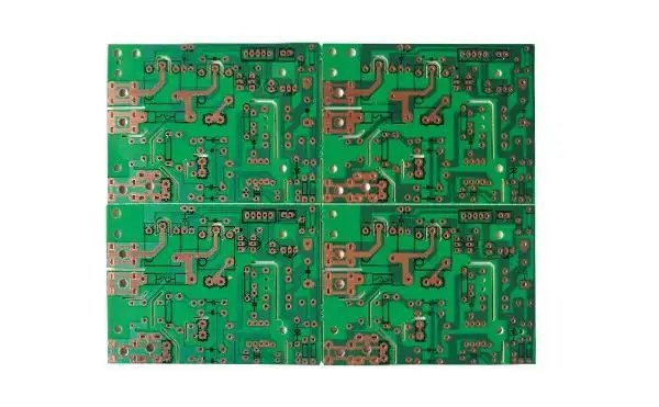
Layout and explanation of circuit board layer in circuit board design
The hierarchical arrangement of the circuit board is quite related to the frequency of the system and the huge wiring of the system. Because of the huge EMI and wiring, 10 layer wiring is adopted. The EMI rules in the cabling from two layers to eight layers are described in detail below.
6.1 Arrangement of two-layer boards
1) The two-layer circuit board is mainly used in low-speed circuits, with operating frequency below 10KHZ or in analog circuits. Its stack level is relatively small and the cost is low.
2) The power trace of two layers of boards is wired in the same layer with radial pull wire from the power supply to each element, reducing the length of all traces.
3) The grid distribution of Power and GND in the two-layer board (distributed in TOP and BOTTOM), because the power noise will go in the direction of low impedance, go in the direction of low impedance from the NOISE source of the power supply, and return to the NOISE source to form a loop. Even though all POWER and GND are adjacent to each other in parallel, the lattice distribution can minimize the loop of noise from high-frequency switching, so it will not affect other circuits and control signals.
4) Another routing method for two-layer boards is that the POWER and signal layers are distributed on one layer and the GND layer is distributed on the other, which can be used when the routing is not dense.
2 Arrangement of four layers of boards
General hierarchical arrangement: TOP and BOTTOM are signal layers, layer 2 is GND, and layer 3 is POWER. The distribution of layer 2 and layer 3 shall be determined according to the specific situation. The layer adjacent to the layer shall be defined as the stratum if it has more routes.
The four layer board is used for medium and low speed lines (below 75M), because there will be a lot of noise in the POWER layer. Therefore, as a reference plane, it is inferior to GND layer.
If the high-speed signal exceeds 66MHZ at the top layer of the four layer board, its high-frequency radiation will radiate to the surrounding. GND must be distributed at the mechanism or top layer to eliminate the radiation.
If the shell is a metal shell, the high-speed signal line and clock line should be placed on a layer close to the shell plane. It is better to lay a circle of ground wire around the clock line, which is 1 to 2 times the width of the clock. It can be as wide as the clock line. If the line is too long, a ground hole should be drilled at an interval of about 1000 mils to enhance the connection between the too long ground wire and the ground and ensure good shielding effect.
IMAGE THEORY:
If a conductor with current is parallel to and adjacent to a metal plane, an image current will be induced on the metal plane in the opposite direction to the same size of the conductor current to offset the radiation field caused by the conductor current. If it is perpendicular to an adjacent metal plane, the image current will be equal in size and direction. Therefore, follow IMAGE THEORY. If there is a signal with high frequency. It is better to complete the wiring in the same layer.
3 Arrangement of six layers
Mode 1: signal layer 1 is the safest wiring mode
Layer 1: signal layer 1.
Layer 2: Land layer.
Layer 3: signal layer 2.
Layer 4: signal layer 3.
Layer 5: power layer.
Layer 6: signal layer 4.
The noise margin of signal layers 2, 3 and 4 is poor, because the magnetic field of POWER PLAN will move through signal layers 2 and 3 to GND PLANE. POWER is not adjacent to GND PLANE, resulting in increased impedance. The signal layers 3 and 4 FLUX CANCELLATION are poor, and the signal layers 2 and 3 have CROSSSTALK concerns.
Because noise will automatically select the loop with the lowest impedance, signal lines and clock lines with high frequency and strong radiation should be as close to the GND layer as possible.
Because the power layer has different partitions, such as 3V, 5V and 12V, the power layer is a broken metal plane, which is also the reason why it is not as good as GND as the reference plane. Therefore, the routing of CLK, SIGNAL and CRYSTAL should be close to the GND layer, that is, the first layer.
Since the noise of POWER will be connected to GND layer, and then returned to POWER layer, the noise will oscillate back and forth between layers 2. Resonance is generated by POWER and GND, generally between 30-230MHZ. The bandwidth of this frequency can only be eliminated by processing POWER and GND. The main method is to eliminate the noise source and improve the signal waveform; Add a capacitor near the high-frequency signal (POWER and GND are connected) to filter the noise from the capacitor.
Method 2:
Layer 1: signal layer 1.
Layer 2: signal layer 2.
Layer 3: Land layer.
Layer 4: power layer.
Layer 5: signal layer 3.
Layer 6: signal layer 4.
Signal layer 2 is adjacent to GND layer, because the mapping theorem has a good FLUX CANCELLATION.
The POWER and GND layers are adjacent to each other to reduce the impedance of the POWER layer.
The FLUX CANNCELLATION of signal layers 1, 3 and 4 is poor, and CROSSSTALK is worried about it.
If the POWER plane has a good reference plane, mode 1 should be selected, because the POWER GND is a good reference plane and there are many layers for high-speed lines. If the POWER layer is broken, mode 2 should be selected. At the same time, mode 2 can be remedied by using GND copper cloth on signal layers 1 and 4.
Mode 3: (the best stacking mode)
Layer 1: signal layer 1.
Layer 2: Land layer.
Layer 3: signal layer 2.
Layer 4: power layer.
Layer 5: signal layer 3.
Layer 6: signal layer 4.
Signal layers 1 and 2 are adjacent to GND layer and have good FLUX CANCELLATION.
In order to avoid the influence of power supply noise in the signal layer, the medium distance between the power layer and the signal layer 2 should be increased to reduce the interference between layers.
Summary: For high-speed signals, it is better to only drill holes at the top and bottom layers, and only one layer in the middle. The existing layers are distributed as follows:
Layer 1: signal layer 1.
Layer 2: Land layer.
Layer 3: power layer.
Layer 4: signal layer 2.
Layer 5: Land layer.
Layer 6: signal layer 3.
Note: The signal layer and POWER layer should be more than 20H smaller than GND layer (H is the distance between POWER GND layers), which can reduce the panel edge radiation by 70%. For our current products, I suggest that the signal layer and POWER layer should be more than 3mm smaller than GND layer.
4 The best arrangement of eight layers
Layer 1: signal layer 1.
Layer 2: Land layer.
Layer 3: signal layer 2.
Layer 4: Land layer.
Layer 5: power layer.
Layer 6: signal layer 3.
Layer 7: Land layer.
Layer 8: signal layer 4.
There are two modes: G2P7 and G3P6.
Disadvantages: With the increase of POWER impedance, there are many signal layers that can be distributed at high speed, which will cause crosstalk between adjacent signal layers.
5 Determine the number of PCB layers before wiring
The number of wiring layers shall be determined at the initial stage of design. If the design requires the use of high-density ball grid array (BGA) components, the minimum number of wiring layers required for the wiring of these devices must be considered. The number of wiring layers and the stacking up method will directly affect the wiring and impedance of the printed wire. The size of the board is helpful to determine the stacking mode and the width of the printed line to achieve the desired design effect.
For many years, people have always believed that the lower the number of circuit boards, the lower the cost. However, there are many other factors that affect the manufacturing cost of circuit boards. In recent years, the cost difference between multilayer boards has been greatly reduced. At the beginning of the design, it is better to use more circuit layers and make the copper coating evenly distributed, so as to avoid that a small number of signals do not meet the defined rules and space requirements when the design is near the end, so that new layers are forced to be added. Careful planning before design will reduce a lot of trouble in cabling. The circuit board processing and PCBA processing manufacturers will explain the arrangement of the circuit board layer of the circuit board design.


Just upload Gerber files, BOM files and design files, and the KINGFORD team will provide a complete quotation within 24h.