
Professional PCB manufacturing and assembly
Building 6, Zone 3, Yuekang Road,Bao'an District, Shenzhen, China
+86-13410863085Mon.-Sat.08:00-20:00

Explanation and analysis of cross division design of PCB
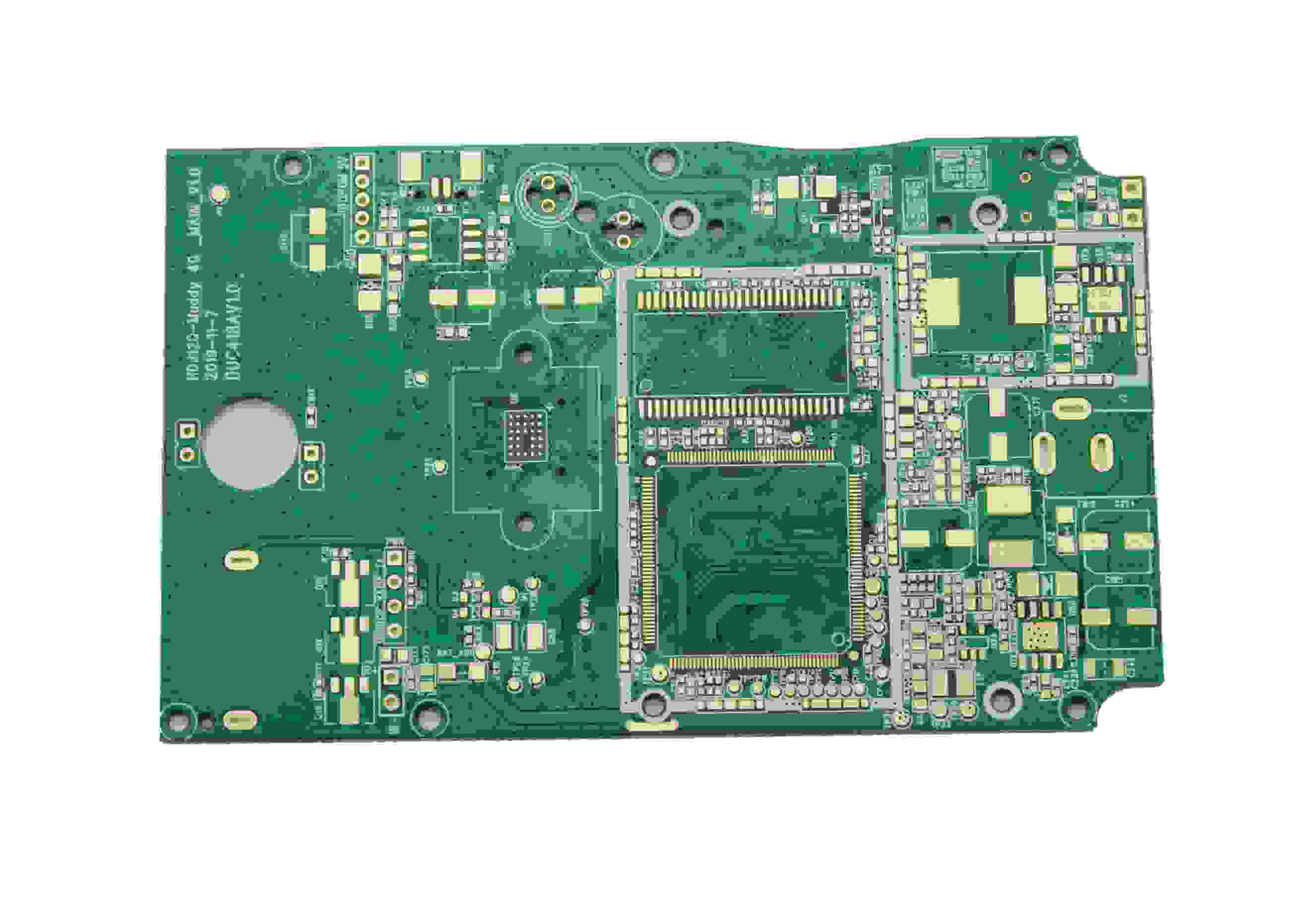
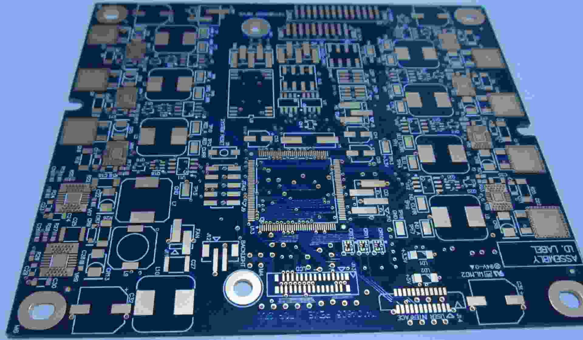
In circuit design, there are more and more multiple power supplies and multiple grounds on a PCB, such as 48V, 12V - 12V, 5V, - 5V, 3.3V, 2.5V, 1.8V1.5V and other common types of power supplies, AGND (analog ground), DGND (digital ground), PGND (protective ground) and other different functions. Some ICs explicitly require the IC to conduct single point grounding, and the required power supply and ground plane are hollowed out. In order to ensure the high reliability of these ground and power supplies, the distribution of each power supply and ground to a layer, that is, a plane, will inevitably lead to the increase of circuit board layers, and the cost of circuit board production will increase significantly. As mentioned earlier, the cost of making a circuit board is proportional to the number of layers. In order to save costs and ensure the reliability of the circuit board, engineers will design the power or ground of two or more PCBs on the same plane according to the characteristics of the circuit board, resulting in incomplete power and ground planes, that is, ground (power) layer segmentation.
1、 Cross division design of PCB board
The PCB wiring on the circuit is divided through the ground (power) layer, and the integrity of the signal will be greatly affected, as well as the EMI and EMC characteristics of the circuit will also change. This is the cross division problem. These are also problems that electronic engineers easily ignore. There are two main sources of cross cutting topics:
1. Division of power/ground plane
On the same layer (stratum), there are analog and digital divisions. When PCB routing passes through this partition band, cross partition problems occur.
2. Segmentation caused by improper definition of pins of dense vias or densely inserted (crimped) devices
If dense vias or dense plug-in (crimping) devices are distributed unfairly during pin definition, and the spacing between pins is very small, a narrow isolation zone will be created in the stratum or definition layer. If a wire runs through this division, it will cause cross division.
These wiring methods are impeccable on the surface: neat and beautiful, which are also the preferred wiring methods of general electronic or circuit engineers. If we look at the power/ground plane of the corresponding area of these vias, we will find that the problem of power and stratum segmentation arises.
Due to the close spacing of vias, a long dividing strip is created on the power/ground plane. If there is a cable running through this partition band, cross partition problems also occur. This kind of problem mainly appears in the bus wiring in the circuit, which must arouse the attention of engineers.
Similarly, when vias (including pads and vias) pass through the ground/power plane, if the spacing between vias is too close, the above problem also occurs. This kind of problem mainly occurs when the definition of pins of densely packed (crimped) devices is not correct. Therefore, when defining pin signals of densely packed (crimped) devices, it is necessary to consider not only the number and type of signals, but also the arrangement of signal buses, so as to avoid cross division problems caused by division of power supply and ground plane.
2、 Hazards of PCB cross split routing
The main hazards of cross split routing include:
(1) Impedance discontinuity of wiring;
(2) It is easy to cause crosstalk between signals;
(3) May cause reflection of signal;
(4) Increase the area and inductance of the current loop, so that the output waveform can easily oscillate;
(5) It increases the radiation interference to the space and is vulnerable to the influence of the space magnetic field;
(6) Increase the possibility of magnetic field coupling with other circuits on the board;
(7) The high frequency voltage drop on the loop inductance forms a common mode radiation source and generates common mode radiation through external cables.
For high-speed signal lines that need strict impedance control and are routed according to the stripline model, the notch on the upper plane, lower plane or upper and lower planes will also destroy the stripline model, resulting in impedance discontinuity, causing serious signal distortion, and reducing the reliability of the signal.
In order to vividly describe the influence of cross split routing on electromagnetic interference, the author has carried out experimental comparison. It is easy to see the impact of cross segmentation from the comparison results. PCBA manufacturers will explain to you the hazards of PCB cross division design, explanation and analysis, power/ground plane division and PCB cross division routing.


Just upload Gerber files, BOM files and design files, and the KINGFORD team will provide a complete quotation within 24h.