
Professional PCB manufacturing and assembly
Building 6, Zone 3, Yuekang Road,Bao'an District, Shenzhen, China
+86-13410863085Mon.-Sat.08:00-20:00

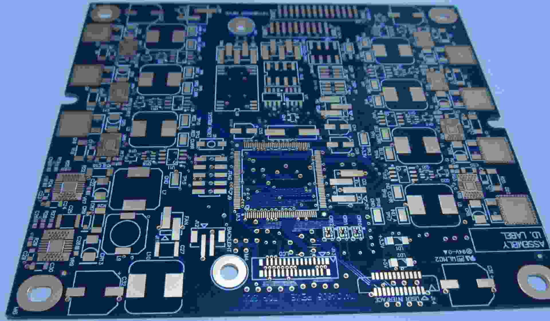
PCB factory: high-speed PCB design sharing based on Cadence
1 Introduction
With the continuous improvement of people's demand for communication, the speed of signal transmission and processing is required to be faster and faster. The corresponding high-speed PCB is also used more and more widely, and the design is more and more complex High speed circuit has two meanings: one is high frequency. It is generally believed that the frequency of digital circuit reaches or exceeds 45MHz to 50MHz, and the circuit working on this frequency has accounted for one third of the whole system, which is called high speed circuit In addition, considering the rise and fall time of the signal, when the rise time of the signal is less than 6 times the signal transmission delay, the signal is considered to be a high-speed signal, and the consideration is independent of the specific frequency of the signal
2 Basic content of high-speed PCB design
The proportion of high-speed circuit design in modern circuit design is getting larger and larger, and the design difficulty is getting higher and higher. Its solution requires not only high-speed devices, but also the wisdom and careful work of designers. We must carefully study and analyze the specific situation to solve the existing high-speed circuit problems Generally speaking, it mainly includes three aspects: signal integrity design, electromagnetic compatibility design and power integrity design
2.1 signal integrity design
Signal integrity refers to the quality of the signal on the signal line A signal with good signal integrity means that it has the required voltage level value when needed Poor signal integrity is not caused by a single factor, but by multiple factors in board level design Especially in high-speed circuits, the switching speed of chips used is too fast, the layout of terminal components is unreasonable, and the interconnection of circuits is unreasonable, which will cause signal integrity problems. Specifically, it includes crosstalk, reflection, overshoot and undershoot, oscillation, signal delay, etc
2.1.1 Crosstalk
Crosstalk is unnecessary coupling between two adjacent signal lines. Mutual inductance and mutual capacitance between signal lines cause noise on the line. Therefore, it is also divided into inductive crosstalk and capacitive crosstalk, which cause coupling current and coupling voltage respectively. When the edge rate of the signal is less than 1ns, crosstalk should be considered If there is an alternating signal current passing through the signal line, an alternating magnetic field will be generated, and the signal voltage will be induced by the adjacent signal lines in the magnetic field In general, the parameters of PCB layer, the distance between signal lines, the electrical characteristics of driver and receiver, and the termination mode of signal lines have certain effects on crosstalk In Cadence's signal simulation tool, six coupled signal lines can be simulated after crosstalk at the same time. The scanning parameters that can be set include: dielectric constant of PCB, thickness of medium, thickness of copper deposit, length and width of signal lines, and spacing of signal lines During simulation, an injured signal line must also be specified, that is, to investigate the interference of other signal lines on this line. The excitation is set to constant high or constant low, so that the sum of the induced voltages of other signal lines on this signal line can be measured, so that the minimum spacing and maximum parallel length that meet the requirements can be obtained
2.1.2 Reflection
The reflection is just like what we know when light passes through discontinuous media, it will reflect some energy back, that is, the echo of the signal on the transmission line. At this time, the signal power is not completely transmitted to the load, and some of it is reflected back In a high-speed PCB, the wire must be equivalent to a transmission line. According to the transmission line theory, if the source end and the load end have the same impedance, reflection will not occur. The impedance mismatch between the two will cause reflection, and the load will reflect part of the voltage back to the source end. Depending on the relationship between the load impedance and the source impedance, the reflected voltage may be positive or negative If the reflected signal is very strong and superimposed on the original signal, it is likely to change the logic state and cause errors in the received data. If the clock signal is not monotonous, it may cause false triggering General wiring geometry, incorrect wire termination, transmission through connectors, and discontinuities in the power plane can cause such reflections In addition, there is often one output and multiple receivers. At this time, the reflection generated by different wiring strategies has different effects on each receiver. Therefore, the wiring strategy is also a factor that cannot be ignored. PCB processing and PCBA processing manufacturers will explain the high-speed PCB design sharing based on Cadence.


Just upload Gerber files, BOM files and design files, and the KINGFORD team will provide a complete quotation within 24h.