
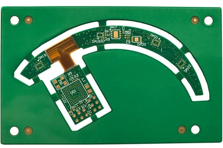
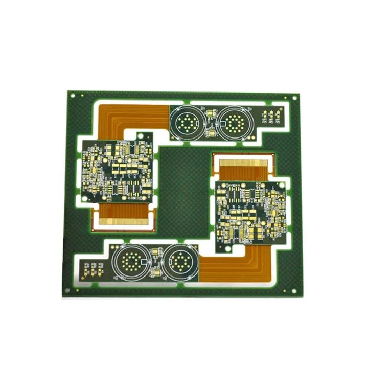
Professional PCB manufacturing and assembly
Building 6, Zone 3, Yuekang Road,Bao'an District, Shenzhen, China
+86-13410863085Mon.-Sat.08:00-20:00

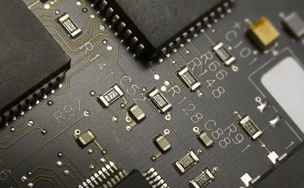
Basis for selecting the wire width of printed PCB: the minimum width of the printed wire is related to the current flowing through the wire: if the wire width is too small, the resistance of the printed wire is large, the voltage drop on the wire is large, which affects the performance of the circuit. If the wire width is too wide, the wiring density is not high, and the board area is increased, except
1: Selection basis of printed wire width:
The minimum width of the printed wire is related to the current flowing through the wire:
If the line width is too small and the resistance of the printed wire is large, the voltage drop on the line will be large, which will affect the performance of the circuit,
If the line width is too wide, the wiring density is not high, and the board area increases. In addition to increasing costs, it is not conducive to miniaturization
If the current load is calculated by 20A/mm2, when the thickness of copper clad foil is 0.5MM, the current load of 1MM (about 40MIL) line width is 1A,
Therefore, the line width of 1 -- 2.54MM (40 -- 100MIL) can meet the general application requirements. The line width of the ground wire and power supply on the high-power equipment board can be appropriately increased according to the power size. For low-power digital circuits, in order to improve the wiring density, the minimum line width of 0.254 -- 1.27MM (10 -- 15MIL) can meet the requirements
In the same circuit board, the power line and ground line are thicker than the signal line
2:
Line spacing: when the line spacing is 1.5 mm (about 60 MIL), the insulation resistance between lines is greater than 20 M Ω, and the maximum withstand voltage between lines can reach 300 V. When the line spacing is 1 mm (40 MIL), the maximum withstand voltage between lines is 200 V. Therefore, on the circuit board of medium and low voltage (the line to line voltage is not greater than 200 V), the line spacing is 1.0 -- 1.5 mm (40 -- 60 MIL). In low-voltage circuits, such as digital circuit systems, the breakdown voltage does not need to be considered, but can be very small as long as the production process allows
3: Pad: For a resistance of 1/8W, a pad lead diameter of 28MIL is sufficient,
For 1/2W, the diameter is 32MIL, the lead hole is too large, and the copper ring width of the PCB pad is relatively reduced, resulting in reduced adhesion of the pad It is easy to fall off, the lead hole is too small, and it is difficult to load components
4: Draw circuit border:
The shortest distance between the border line and the component pin pad shall not be less than 2MM (generally, it is reasonable to take 5MM), otherwise blanking is difficult
5: Element layout principle:
A General principle: In PCB design, if the circuit system has digital circuit and analog circuit at the same time As well as large current circuits, they must be laid out separately to minimize the coupling between systems. In the same type of circuit, components must be placed in blocks and zones according to the signal flow direction and function
B: Input signal processing unit and output signal driving element shall be close to the circuit board edge to make input and output signal lines as short as possible to reduce input and output interference
C: Component placement direction: components can only be arranged horizontally and vertically. Otherwise, they cannot be placed in the plug-in
D: Element spacing For medium density boards, small components, such as small power resistors, capacitors, diodes, and equal split components, the spacing between them is related to the plug-in and PCB welding process. During wave soldering, the component spacing can be 50-100MIL (1.27-2.54MM), which can be larger manually. For integrated circuit chips, the component spacing is generally 100-150MIL
E: When the potential difference between components is large, the spacing between PCB components should be large enough to prevent discharge
F: The de coupling capacitor in the IC should be close to the power supply ground wire pin of the PCB chip, otherwise the filtering effect will become worse In the digital circuit, in order to ensure the reliable operation of the digital circuit system, the IC decoupling capacitor is placed between the power supply and the ground of each digital integrated circuit chip. The decoupling capacitor is generally a ceramic chip capacitor, and the capacity of 0.01~0.1UF decoupling capacitor is generally selected according to the reciprocal of the system operating frequency F In addition, a 10UF capacitor and a 0.01UF ceramic chip capacitor shall be connected between the power line and the ground wire at the inlet of the circuit power supply
G: The clock circuit component shall be close to the clock signal pin of the single chip microcomputer chip as far as possible to reduce the connection length of the clock circuit


Just upload Gerber files, BOM files and design files, and the KINGFORD team will provide a complete quotation within 24h.