
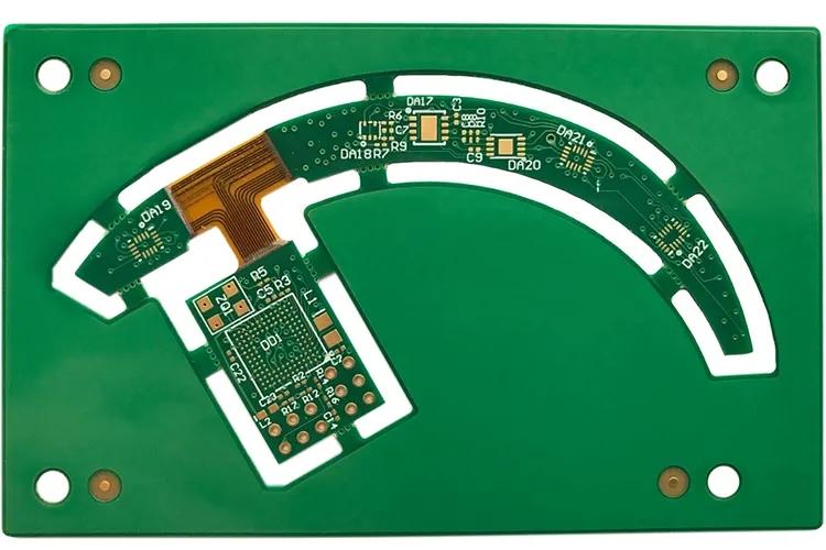
Professional PCB manufacturing and assembly
Building 6, Zone 3, Yuekang Road,Bao'an District, Shenzhen, China
+86-13410863085Mon.-Sat.08:00-20:00

Introduction to high-speed USB design considerations in PCB design
Placement of devices
1. Keep some clock related devices such as clock synthesizer, clock buffer, crystal and crystal oscillator away from the high-speed USB controller and its related cabling, and keep these clock devices away from the I/O port and power connector.
2. Devices such as crystal oscillator and crystal should be placed as close to the PCB surface as possible. If there is a large ground pad, the pad should be connected to GND through multiple vias.
3. Place high current devices close to the power supply and away from connectors as far as possible, so as to reduce the return path of high current and thus reduce electromagnetic radiation.
High speed USB signal termination
1. If the main controller has used an external termination resistor, ensure that the distance between the termination resistor and the signal output pin of the main controller is less than 200 mils.
2. During EMI testing, sometimes a common mode blocker may be placed. At this time, please place it as close to the connector as possible.
3. At the downstream port, ensure that there is a 15K Ohm pull-down resistor between the termination resistor and the USB connector pin.
High speed USB signal wiring
1. Place the high-speed USB host controller and some related main devices before distributing the boards.
2. The differential signal lines are laid side by side.
3. Shorten the routing length as much as possible, give priority to the wiring of high-speed clock signal and high-speed USB differential line, and try to avoid high-speed clock signal and high-speed USB differential line and any connector being close to the routing.
4. Do not walk the signal line under the IC of crystal oscillator, crystal, clock synthesizer, magnetic device and clock frequency multiplication.
5. If possible, let the USB high-speed signal be laid on the bottom layer of the PCB.
6. Try to reduce the number of vias and corners on the USB high-speed signal line, so as to better control the impedance and avoid signal reflection.
7. Avoid short lines on the signal line, otherwise it will cause reflection of the signal, thus affecting the integrity of the signal. If this short line is unavoidable, make sure its length does not exceed 200 mils.
8. The line is laid on a complete plane (VCC or GND), and the lower plane of the existing line has not been divided. If possible, do not cross Anti Etch, otherwise self inductance coefficient and signal radiation will be increased. Similarly, the high-speed signal lines shall be laid in the same layer as far as possible.
9. If a 90 degree turn is unavoidable, use two 45 degrees to achieve the turn or an arc to achieve the turn, which will greatly reduce the signal reflection and impedance discontinuity.
Spacing of high-speed USB cabling
1. The wiring spacing between parallel USB differential signal pairs shall ensure a differential impedance of 90 ohms.
2. Based on some simulation data, the minimum distance between parallel high-speed USB differential signal lines is controlled at more than 20 mils, which will help reduce the crosstalk between high-speed USB differential pairs.
3. Shorten the length of high-speed USB signal line, high-speed clock line and AC signal line side by side, or increase the space between them side by side to reduce the impact of crosstalk. In the EMI test experiment, the reliable minimum spacing is 50 mils.
Matching of high-speed USB cable length
1. When the differential distribution line of the high-speed USB signal is used, the length of the routing should match. The maximum length difference (such as the length difference between DM1 and DP1) cannot be greater than 200 mils.
Requirements for total length of high-speed USB cable
1. Make sure that the total length from the cable to the backplane connector is controlled at 18 inches.
2. Make sure that the total length of the cabling plus the total length of the cable to the USB connector board does not exceed 18 inches. Circuit board assembly and circuit board processing manufacturers explain high-speed USB design considerations for circuit board design.
Explore some operations in PCB design
Dec 03,2022


Just upload Gerber files, BOM files and design files, and the KINGFORD team will provide a complete quotation within 24h.