
Professional PCB manufacturing and assembly
Building 6, Zone 3, Yuekang Road,Bao'an District, Shenzhen, China
+86-13410863085Mon.-Sat.08:00-20:00

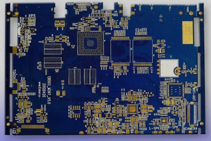
Mobile phone circuit board RF RF PCB chip power decoupling and electrical zoning
RF circuit board design is often described as a "black art" because of many uncertainties in theory, but this view is only partially correct. RF circuit board design also has many rules that can be followed and should not be ignored. The following summarizes the conditions that must be met when designing RF layout of mobile phone PCB board.
1. Proper and effective chip power decoupling is also very important.
Many RF chips integrated with linear circuits are very sensitive to power supply noise. Generally, each chip needs to use up to four capacitors and an isolation inductor to ensure filtering out all power supply noise. An integrated circuit or amplifier often has an open drain output, so a pull-up inductor is required to provide a high impedance RF load and a low impedance DC power supply. The same principle applies to decoupling the power supply at this inductor end. Some chips require multiple power supplies to work, so you may need two or three sets of capacitors and inductors to decouple them respectively. The inductors are rarely placed together in parallel, because this will form an empty core transformer and induce each other to generate interference signals. Therefore, the distance between them should be at least equal to the height of one of the devices, or they should be arranged at right angles to minimize their mutual inductance.
1. The principle of electrical partition is basically the same as that of physical partition, but it also includes some other factors.
Some parts of the mobile phone use different working voltages and are controlled by software to extend the battery life. This means that the phone needs to run multiple power supplies, which brings more problems to isolation. The power supply is usually introduced from the connector, and is immediately decoupled to filter out any noise from outside the circuit board, and then distributed after passing through a group of switches or regulators. The DC current of most circuits on the mobile phone PCB is relatively small, so the wiring width is usually not a problem. However, a large current line as wide as possible must be separately routed for the power supply of the high-power amplifier to minimize the transmission voltage drop. To avoid too much current loss, multiple vias are required to transfer current from one layer to another. In addition, if it cannot be fully decoupled at the power supply pin end of the high power amplifier, the high power noise will radiate to the whole board and cause various problems. The grounding of high power amplifier is very important, and it is often necessary to design a metal shield for it. In most cases, it is also critical to ensure that the RF output is kept away from the RF input. This also applies to amplifiers, buffers, and filters. In the worst case, if the outputs of amplifiers and buffers are fed back to their inputs with appropriate phase and amplitude, they may generate self-excited oscillation. In the best case, they will be able to work stably under any temperature and voltage conditions. In practice, they may become unstable and add noise and intermodulation to the RF signal. If the RF signal line has to bypass the input end of the filter back to the output end, it may seriously damage the bandpass characteristics of the filter. In order to achieve good isolation between input and output, a circle of ground must be laid around the filter first, and then a piece of ground must be laid in the lower layer of the filter, and connected with the main ground around the filter. It is also a good method to keep the signal wire that needs to pass through the filter as far away from the filter pin as possible.
In addition, the grounding of the whole board should be very careful, otherwise a coupling channel will be introduced. Sometimes you can choose to use single ended or balanced RF signal lines. The principles of cross interference and EMC/EMI are also applicable here. Balanced RF signal lines can reduce noise and cross interference if they are routed correctly, but their impedance is usually high. To maintain a reasonable line width to obtain an impedance that matches the signal source, routing and load, actual wiring may have some difficulties. Buffer can be used to improve isolation effect, because it can divide the same signal into two parts and drive different circuits. In particular, local oscillator may need buffer to drive multiple mixers. When the mixer reaches the common mode isolation state at RF frequency, it will not work properly. Buffer can well isolate impedance changes at different frequencies, so that circuits will not interfere with each other. Buffers are very helpful for design. They can closely follow the circuit to be driven, so that the high power output wiring is very short. Because the input signal level of the buffer is low, they are not easy to interfere with other circuits on the board. Voltage controlled oscillators (VCOs) can convert varying voltages into varying frequencies, which is used for high-speed channel switching. However, they also convert the small noise in the control voltage into small frequency changes, which adds noise to RF signals. PCB assembly, PCB design and PCBA processing manufacturers will explain the power decoupling and electrical zoning of RF RF PCB chips of mobile phone circuit boards.


Just upload Gerber files, BOM files and design files, and the KINGFORD team will provide a complete quotation within 24h.