
Professional PCB manufacturing and assembly
Building 6, Zone 3, Yuekang Road,Bao'an District, Shenzhen, China
+86-13410863085Mon.-Sat.08:00-20:00

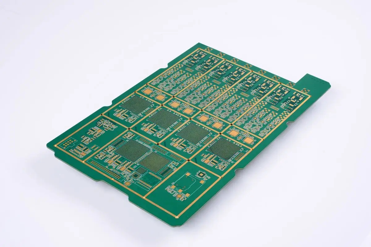
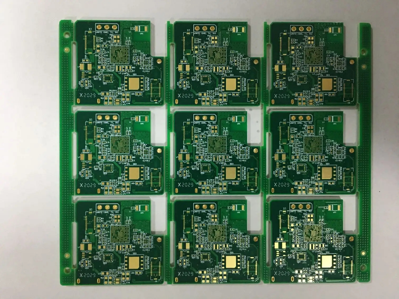
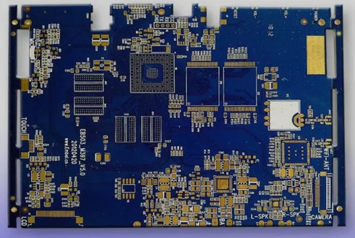
Layout and wiring of RF RF PCB board for mobile phones in circuit board factory
The circuit board processing factory summarizes the conditions that must be met when designing RF layout of mobile phone PCB.
RF circuit board design is often described as a "black art" because of many uncertainties in theory, but this view is only partially correct. RF circuit board design also has many rules that can be followed and should not be ignored. The following summarizes the conditions that must be met when designing RF layout of mobile phone PCB board.
However, in actual design, the real practical skill is how to compromise these rules and regulations when they cannot be implemented accurately due to various design constraints. Of course, there are many important RF design topics worth discussing, including impedance and impedance matching, insulating layer materials and laminates, and wavelength and standing wave. Therefore, these have a great impact on the EMC and EMI of mobile phones. Here is a summary of the conditions that must be met when designing the RF layout of mobile phone PCB.
1.1 Isolate high power RF amplifier (HPA) and low noise amplifier (LNA) as much as possible.
In short, it is to keep the high power RF transmitting circuit away from the low power RF receiving circuit. Mobile phones have many functions and components, but the PCB space is small. Considering that the design process of wiring is the most limited, all these require high design skills. At this time, it may be necessary to design four to six layers of PCBs so that they can work alternately instead of simultaneously. High power circuits can sometimes include RF buffers and voltage controlled oscillators (VCO). Make sure that the high power area on the PCB has at least one whole ground. It is better to have no via on it. Of course, the more copper sheets, the better. Sensitive analog signals should be as far away from high-speed digital signals and RF signals as possible.
1.2 The design partition can be divided into physical partition and electrical partition.
Physical zoning mainly involves the layout, orientation and shielding of components; The electrical partition can be further divided into power distribution, RF wiring, sensitive circuits and signals, and grounding partitions.
1.2.1 We discuss physical zoning.
Component layout is the key to an excellent RF design. The most effective technology is to first fix the components on the RF path, and adjust their orientation to minimize the length of the RF path, keep the input away from the output, and separate the high power circuit and low power circuit as far as possible.
The most effective circuit board stacking method is to arrange the main ground (main ground) on the second layer below the surface layer, and try to lay the RF line on the surface layer. Minimizing the size of vias on the RF path can not only reduce the path inductance, but also reduce the number of solder joints on the main ground, and reduce the chance of RF energy leakage to other areas in the laminate. In physical space, linear circuits such as multistage amplifiers are usually sufficient to isolate multiple RF regions from each other, but duplexers, mixers, and IF amplifiers/mixers always have multiple RF/IF signals interfering with each other, so care must be taken to minimize this impact.
1.2.2 RF and IF wiring shall be crossed as far as possible and separated from each other by a piece of land as far as possible.
The correct RF path is very important for the performance of the whole PCB, which is why component layout usually takes up most of the time in mobile phone PCB design. In the design of mobile phone PCB board, it is usually possible to place the low-noise amplifier circuit on one side of the PCB board and the high-power amplifier on the other side, and finally connect them on the same side to the RF and baseband processor antennas through the duplexer. Some techniques are required to ensure that the through vias do not transfer RF energy from one side of the board to the other. The common technique is to use blind holes on both sides. The adverse effects of the through vias can be minimized by arranging them in the area where both sides of the PCB are free from RF interference. Sometimes it is impossible to ensure sufficient isolation between multiple circuit blocks. In this case, it is necessary to consider the use of a metal shield to shield RF energy in the RF area. The metal shield must be welded to the ground and must be kept at an appropriate distance from the components. Therefore, it needs to occupy valuable PCB space. It is very important to ensure the integrity of the shield as much as possible. The digital signal line entering the metal shield should go through the inner layer as much as possible, and the PCB below the line layer should be the layer. RF signal lines can go out from the small gap at the bottom of the metal shield and the wiring layer at the ground gap, but more ground should be laid around the gap as much as possible, and the ground on different layers can be connected together through multiple vias.


Just upload Gerber files, BOM files and design files, and the KINGFORD team will provide a complete quotation within 24h.