
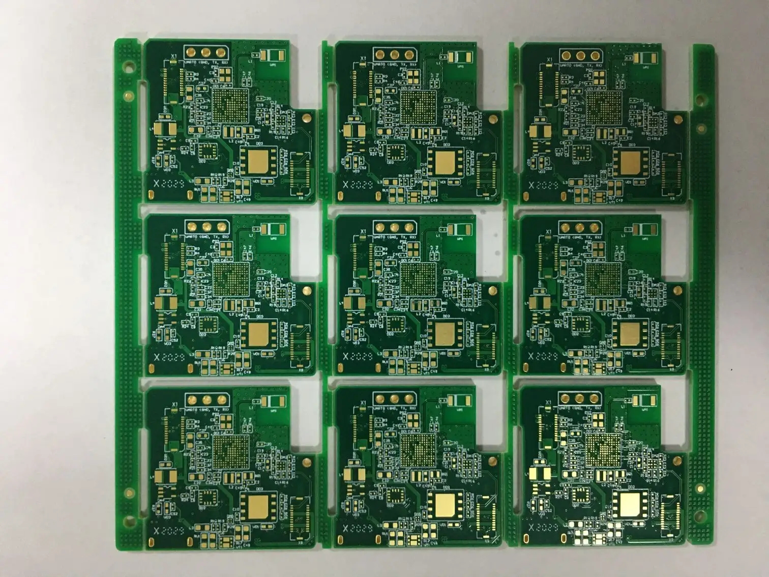
Professional PCB manufacturing and assembly
Building 6, Zone 3, Yuekang Road,Bao'an District, Shenzhen, China
+86-13410863085Mon.-Sat.08:00-20:00

Key inspection part of mobile phone PCB layout and routing design
1. Device package inspection
We need to carefully check the packaging of motherboard components to avoid errors. Especially for new materials used in the project, PCB packaging must be carefully checked with reference to the spec.
2. Layout of components
When stacking, it is necessary to consider the layout of structural parts and main components, such as I/O connector, SIM card, battery connector, T card, camera, speaker, receiver, RF part, baseband part, GSM antenna part, Bluetooth antenna part, mobile TV antenna part. In addition to ID and MD, the placement of these parts also needs to consider the mutual influence.
In the MTK scheme, SIM cards and buttons are easy to be interfered by the GSM antenna, so it is necessary to keep away from the GSM antenna as far as possible. GSM antenna area, Bluetooth antenna area and mobile TV antenna area all need a suitable area. If the GSM is used as a PIFA antenna, it needs an area of 500mm2 and a height of more than 5mm from the antenna to the motherboard. There should be no I/O connector, T card, speaker and other devices under the antenna, otherwise the height can only be calculated according to the height from the device below to the antenna; If Monopole is used, the antenna space needs 30mm × 10mm, the ground in this area on the motherboard shall be hollowed out, and the projection surface between the antenna and the motherboard shall be free of metal. The speaker and receiver are vulnerable to antenna interference, resulting in TDMA noise
, the relative position between them and the antenna needs to be considered. The battery connector to the PA power supply also needs to be short. The RF part can be used as a proper whole to lay down the IQ line, 26MHZ signal line and control line from the RF part to the baseband part in the shielding cover position given by Stacking. The control line should be as short and as smooth as possible. For the layout of the RF part, it is necessary to straighten out the RX receiving line from the FEM to the transmitter, the TX transmitting line from the transmitter to the PA, and the TX transmitting line from the PA to the FEM or ASM.
The small filter capacitor of the power supply network should be as close to the chip pin as possible to reduce the lead inductance. Other components shall be placed according to the principle of proximity and passing. The placement of components shall also consider the height limit. In addition to the height limit on the structure, the height of the shielding cover will also limit the placement of components. At present, the height of the two-piece shield is 1.8mm, and the height of the one-piece shield is 1.6mm. The height of the components in the RF shield must be within this range. If it is close to the periphery of the shield, or on the ribs of the shield, the height will be more limited. The height of the main chips in the RF part is 1.4mm, the height of FEM NTK5076 is 1.8mm, and the height of IMT0103B is 1.6mm. 47UF tantalum capacitor is 1.8mm high.
3. Routing definition of each layer
Before routing, we need to determine the main stratum and power layer, and generally plan which layer the data line, IQ line, impedance line, audio line, high-frequency signal line, control line and so on should go to.
Take the common 8-layer single-stage RF part single-sided pendulum motherboard as an example. The eighth layer is for device placement, the first layer is not for placement, the sixth layer is for secondary ground, and the fourth layer is for primary ground,. The power and data lines shall be routed to the second and third layers, and the TX and RX impedance lines shall be routed to the eighth layer as far as possible, and the seventh layer shall be hollowed out, refer to the sixth layer. Layer 7 shall not be wired as much as possible. IQ lines, audio lines, AFC, APC, 26MHZ, impedance lines, etc. are relatively vulnerable to interference. Those that need special grounding can go to Layer 5. The upper and lower layers need grounding. The fourth floor is the main ground, and the sixth floor is the auxiliary ground. Try not to route.
4. Wiring specification
4.1 Impedance line
The impedance line shall be laid on the surface layer as far as possible. When laying on the surface layer, the lower layer shall be hollowed out, and then the lower layer shall be used as the reference ground. When walking on the inner floor, the upper and lower floors need to be covered, and the left and right sides also need to be well covered. The first and eighth layers of the 27 holes should be on the ground. Keep away from data lines, power lines and signal lines to avoid interference. Both TX impedance lines control 50ohm, while RX impedance lines currently run on 150ohm differential lines. RX differential impedance control lines shall be parallel, close and equal in length.
4.2 High frequency signal line
High frequency signal lines, such as 26MHZ, EDCLK, etc., shall be specially protected to avoid interference with GSM reception. Try to go inside and the shortest distance. The upper and lower floors need to be covered. If 27 holes need to be drilled, make sure that the 1st and 8th layers at the 27 hole location are on the ground. High frequency signal line shall not walk near the antenna area.
4.3 APC, AFC, IQ lines and control lines to be protected
The IQ cable should be specially protected, and it usually goes through the middle layer, such as the fifth layer. The upper and lower floors should be on the ground. The left and right sides shall be covered with copper for protection. Try to keep away from interference sources, such as power lines, data lines, high-frequency signal lines, etc. At the same time, 27 holes of the above interference sources should be avoided, which are too close to the IQ line. Since the IQ line is a difference line, it needs to be parallel, close and equal in length. The IQ line should be straight and the shortest distance. APC and AFC need to be separately covered, and the upper and lower floors need to be covered. Keep away from interference sources. Other control lines, such as PA band select, PA enable, and FEM band select, can be run together to cover the ground as much as possible, and also be far away from interference sources as much as possible.
4.4 Power supply and ground
It is very important to route the power supply on the motherboard. Try to make the entire power network a star type instead of an O type power network, forming a power circuit and reducing EMC performance. When PA works, it consumes a lot of current. In order to avoid too large voltage drop of PA input power supply, the power supply line of PA must be thick, and generally the line width is 80 mil. More mechanical holes and laser holes shall be drilled when changing layers. Make it fully connected, and more holes shall be punched at the connection with the battery connector. The power cord of VCCA and VCCB pin pin of PAsky77328 of Skyworks shall be pulled out separately from the battery connector, with a wire width of at least 16mil. The power supply to the transmitter also needs to be pulled out separately from the battery connector, with a line width of 16mil.. The 26mhz crystal oscillator power supply is output from PMU, and also needs to be protected by grounding, with a line width of 12ml. Other AVDD, DVDD, VCCRF, etc. can travel 12 mils. Except for PA power supply, other power lines shall have at least 2 holes when changing layers. All power lines are interference sources, so they cannot be close to the lines or devices that are easy to be interfered. It is also not allowed to be close to the high-frequency signal line, otherwise the high-frequency signal interference will spread all over the motherboard along with the power line.
The ground of the battery connector and the ground of the motherboard should be fully connected. Large holes should be punched to the main ground as much as possible to make it directly connected to the main ground. The more small holes, the better, to ensure that the ground of each layer of the motherboard can fully form a ground loop near the battery connector. Large holes shall also be drilled near the power line to the main ground as much as possible to make the loop area smaller and improve EMC performance. Small holes and large holes shall be drilled at the bonding pad of the shielding frame to fully connect it with the main ground. Large and small holes shall be punched at the edge of the board as much as possible to improve EMC performance. The PAD under PA, FEM and transducer shall be drilled with large and small holes to fully connect with the main ground and be beneficial to PA heat dissipation. Large and small holes shall be drilled under the 26MHZ crystal oscillator pad.
There are several areas where copper laying is prohibited.
1. GSM, BLUETOOTH, mobile TV and other antenna crash point PADs are prohibited to lay copper on layers 1 to 8. If the Monopole antenna is used, it is forbidden to lay copper on layers 1 to 8 of the entire antenna area.
2. There is no need to lay copper on the inner surface of the RF shielding frame. If the RF device is placed on the eighth layer, the ground of the seventh layer is disconnected along the shielding frame and the outer ground, and is directly connected to the main ground by the big hole.
3. The ground below the 26MHZ crystal oscillator is also separated from the surrounding ground and connected to the main ground directly by the large hole.
In a word, the more ground holes, the better. However, if too many holes are densely punched in a large area without wiring, the board factory may have a problem, which leads to the failure of PCB engineering confirmation.
5. Producibility inspection
Check whether the components in the shield cover are too close to the shield cover, which will cause short circuit. The safety distance is 12 mils.
Check whether the device is too close to the edge of the plate, which is easy to drop.
Check the solder mask layer, antenna pad, speaker PAD, RECEIVER PAD, vibration motor PAD, etc. to determine whether to tin.
Next, we attach a series of notes:
1. The RX line is a 150 ohm differential impedance line. The line width shall be adjusted according to the actual situation. It is required that the two lines are parallel, close and equal in length.
2. The TX line is a 50ohm impedance line, and the line width is adjusted according to the actual situation.
3. The power supply of PA is 80 mil, and more holes shall be drilled when changing floors. At least 2 large holes and 4 small holes.
4. For PA VCCA and VCCB, a single wire with a width of 16mil shall be connected from the battery connector.
5. For the 6129 power supply, a separate wire with a width of 16mil is required from the battery connector.
6. IQ cable: 6mil, covering the ground from top to bottom, left to right. They need to be parallel, close and equal in length.
7. APC and AFC should be covered for 4mil. Other control lines shall be laid for 4mil, and the ground shall be covered as far as possible.
8. More ground holes shall be drilled under FEM, PA and transmitter.
9. Other RF power cables are 16mil long. When changing layers, two small holes are required.
The 10,26MHZ signal line runs for 4mil and needs to be well grounded. PCB assembly, PCB design and PCBA manufacturer will explain the key inspection parts of mobile phone PCB layout and wiring design.


Just upload Gerber files, BOM files and design files, and the KINGFORD team will provide a complete quotation within 24h.