
Professional PCB manufacturing and assembly
Building 6, Zone 3, Yuekang Road,Bao'an District, Shenzhen, China
+86-13410863085Mon.-Sat.08:00-20:00

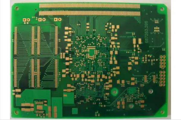
PCB mobile phone RF RF PCB board ensures no increase in noise
RF circuit board design is often described as a "black art" because of many uncertainties in theory, but this view is only partially correct. RF circuit board design also has many rules that can be followed and should not be ignored. The following summarizes the conditions that must be met when designing RF layout of mobile phone PCB board.
The following aspects must be considered to ensure no noise increase:
First, the expected bandwidth of the control line may range from DC to 2MHz, and it is almost impossible to remove such broadband noise through filtering; Secondly, VCO control line is usually a part of a feedback loop that controls frequency. It may introduce noise in many places. Therefore, VCO control line must be handled with great care. It is necessary to ensure that the ground below the RF wiring is solid, and all components are firmly connected to the main ground and isolated from other wiring that may cause noise.
In addition, to ensure that the power supply of VCO has been fully decoupled, VCO must pay special attention to VCO because the RF output of VCO is often a relatively high level, and VCO output signals are easy to interfere with other circuits. In fact, VCO is often placed at the end of RF area, and sometimes it needs a metal shield. Resonant circuit (one for transmitter and the other for receiver) is related to VCO, but it also has its own characteristics. In brief, the resonant circuit is a parallel resonant circuit with capacitive diodes, which is helpful to set VCO operating frequency and modulate voice or data to RF signals. All VCO design principles also apply to resonant circuits. Resonant circuits are usually very sensitive to noise because they contain a large number of components, have a wide distribution area on the board, and usually operate at a very high RF frequency. The signals are usually arranged on the adjacent pins of the chip, but these signal pins need to work with relatively large inductors and capacitors, which in turn requires that these inductors and capacitors must be close together and connected back to a noise sensitive control loop. It is not easy to do this.
Automatic gain control (AGC) amplifier is also a problem prone place, no matter the transmitting or receiving circuit will have AGC amplifier. Generally, AGC amplifiers can effectively filter out noise. However, because mobile phones have the ability to handle the rapid changes in the strength of transmitted and received signals, AGC circuits are required to have a fairly wide bandwidth, which makes it easy for AGC amplifiers on some key circuits to introduce noise. The design of AGC circuit must comply with good analog circuit design technology, which is related to the short input pin of the op amp and the short feedback path, both of which must be far away from RF, IF or high-speed digital signal wiring. Similarly, a good grounding is also essential, and the power supply of the chip must be well decoupled. If it is necessary to run a long line at the input or output end, it is better to run it at the output end. Usually, the impedance of the output end is much lower, and it is not easy to induce noise. Generally, the higher the signal level, the easier it is to introduce noise into other circuits. In all PCB designs, it is a general principle to keep digital circuits away from analog circuits as much as possible, which is also applicable to RFPCB design. Common analog ground and ground used for shielding and separating signal lines are usually equally important.
Therefore, in the early stage of design, careful planning, careful consideration of component layout and thorough layout * evaluation are very important. Also, RF lines should be kept away from analog lines and some very critical digital signals. All RF lines, pads and components should be filled with grounding copper as much as possible and connected to the main ground as much as possible. If the RF wiring must pass through the signal wire, try to lay a layer of ground connected to the main ground along the RF wiring between them. If it is not possible, make sure they are crisscross, which can minimize capacitive coupling. At the same time, try to lay more ground around each RF cable and connect them to the main ground. In addition, the inductive coupling can be minimized by minimizing the distance between parallel RF routes. When a solid whole ground is directly placed on the first layer below the surface, the isolation effect is the best, although other methods can also be used when designing with care. Each layer of PCB shall be laid with as many floors as possible and connected to the main floor. Keep the routing together as much as possible to increase the number of plots in the internal signal layer and power distribution layer, and adjust the routing appropriately so that you can arrange the ground connection vias to the isolated plots on the surface. The generation of free ground on each PCB layer should be avoided, because they will pick up or inject noise like a small antenna. In most cases, if you can't connect them to the main site, you'd better remove them. The circuit board assembly, circuit board design, and circuit board processing manufacturer explain that the RF RF PCB board of the circuit board mobile phone ensures no increase in noise.


Just upload Gerber files, BOM files and design files, and the KINGFORD team will provide a complete quotation within 24h.