
Professional PCB manufacturing and assembly
Building 6, Zone 3, Yuekang Road,Bao'an District, Shenzhen, China
+86-13410863085Mon.-Sat.08:00-20:00

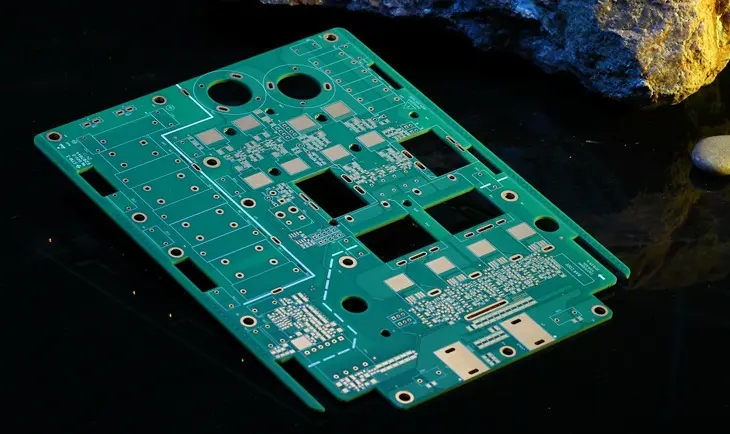
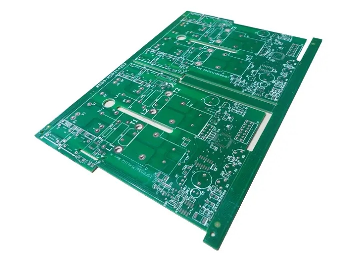
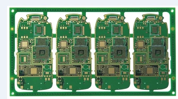
High speed PCB design uses multi-layer and via in proofing
Multilayer circuit boards are recommended for high-speed PCB design. First, the multilayer circuit board allocates the inner layer to power and ground, so it has the following advantages:
·The power supply is very stable;
·The circuit impedance is greatly reduced;
·The wiring length is greatly shortened.
In addition, from the perspective of cost, although the cost of multilayer circuit boards is higher than that of single-layer circuit boards when comparing the cost of the same area, the cost difference between multilayer circuit boards and single-layer circuit boards is not as high as expected when considering other factors such as the miniaturization of circuit boards and the convenience of noise reduction. When we simply calculate the area cost of circuit boards according to the data we know, the area of double-layer circuit boards available for purchase per day is about 462mm2, and the area of 4-layer circuit boards is 26mm2, which means that the same circuit is designed. If the area of 4-layer circuit boards can be reduced to 1/2 of that of double-layer circuit boards, then the cost is the same as that of double-layer circuit boards. Although multiple layers in batches will affect the cost per unit area of the circuit board, there will not be 4 times the price difference. If more than 4 times the price difference occurs, as long as we can try to reduce the use area of the circuit board and try to reduce it to less than 1/4 of the double-layer board.
Through hole design in high-speed PCB proofing
The vias in high-speed PCB are mostly designed by analyzing the parasitic characteristics of vias. We can see that in the process of high-speed PCB design, the seemingly simple vias usually bring great negative effects to the circuit design.
Therefore, in order to reduce the adverse effects caused by the parasitic effect of vias, we can try to do the following in the design:
1. No matter from the point of view of cost and signal quality, choose a reasonable hole size. For example, for the 6-10 layer memory module PCB design, it is better to select 10/20Mil (drill/pad) vias. For some small high-density circuit boards
You can also try to use 8/18Mil vias. Under the current technical conditions, it is more difficult to use the smaller size of the hole. For the via of power supply or ground wire, the larger size can be considered to reduce the impedance.
2. From the discussion of the above two formulas, it can be concluded that the use of thinner PCB is conducive to reducing the two parasitic parameters of vias.
3. The signal line has not changed on the PCB layer, that is to say, do not use unnecessary vias as much as possible.
4. The pins of the power supply and the ground should be punched nearby. The shorter the lead between the via and the pin, the better, because they will increase the inductance. At the same time, the power and ground leads should be as thick as possible to reduce impedance.
5. Place some grounded vias near the vias for signal layer change to provide the latest signal circuit. You can even place a large number of redundant grounding vias on the PCB. Of course, flexible design is also required.
What is discussed above about via model is that when everyone has pads, sometimes we can reduce some layers of keyboards or even cancel them. Especially in the case of very high through-hole density, it may lead to the formation of a circuit breaking groove in the copper layer,
To solve this problem, in addition to moving the position of the via, you can also consider the through-hole on the pad to reduce the size of the copper layer. PCB processing, PCB assembly, PCB design, and PCBA processing manufacturers explain why high-speed PCB design is recommended to use multi-layer PCB and what is the implementation of via design in high-speed PCB proofing.


Just upload Gerber files, BOM files and design files, and the KINGFORD team will provide a complete quotation within 24h.