
Professional PCB manufacturing and assembly
Building 6, Zone 3, Yuekang Road,Bao'an District, Shenzhen, China
+86-13410863085Mon.-Sat.08:00-20:00

Experience summary of anti-interference design in circuit board design
The design of printed circuit board is based on the circuit schematic diagram to realize the functions required by the circuit designer. The design of printed circuit board mainly refers to layout design, which needs to consider the layout of external connections. The optimal layout of internal electronic components, the optimal layout of metal wiring and through-hole, electromagnetic protection, heat dissipation and other factors. Excellent layout design can save production costs and achieve good circuit performance and heat dissipation. Simple layout design can be realized by hand, while complex layout design needs to be realized by computer aided design (CAD)
Software:
1. It is customary to clear all unused code spaces to "0", because this is equivalent to NOP, which can be returned when the program runs;
2. Add several NOPs before the jump instruction, with the same purpose as 1;
3. When there is no hardware WatchDog, software can be used to simulate the WatchDog to monitor the operation of the program;
4. When dealing with the parameter adjustment or setting of external devices, the parameters can be re sent regularly to prevent the external devices from making errors due to interference, so that the external devices can recover correctly as soon as possible;
5. For anti-interference in communication, the data check bit can be added, and the two out of three or three out of five strategy can be adopted;
6. When there are communication lines, such as I ^ 2C, three wire system, etc., in practice, we find that the Data line, CLK line and INH line are normally set to high, and their anti-interference effect is better than low.
Hardware:
1. Wiring of ground wire and power wire
2. Decoupling of lines;
3. Separation of digital and analog ground;
4. Each digital element needs 104 capacitors between the ground and the power supply;
5. To prevent crosstalk of I/O ports, I/O ports can be isolated by diode isolation, gate circuit isolation, optocoupler isolation, electromagnetic isolation, etc;
6. In relay applications, especially when there is a large current, to prevent the interference of relay contact sparks on the circuit, a 104 and a diode can be connected between the relay coils, and 472 capacitors can be indirectly connected between the contact and the normal starting point. The effect is good!
7. Of course, the interference resistance of the multilayer board is certainly better than that of the single panel, but the cost is several times higher.
8. Choosing a device with strong anti-interference capability is more effective than any other method. I think this should be the most important. Because it is difficult to make up for the inherent shortcomings of devices with external methods, but the ones with strong anti-interference ability are often more expensive, and the ones with poor anti-interference ability are cheaper, just like Taiwan's cheap ones with greatly reduced performance! It mainly depends on your application occasions
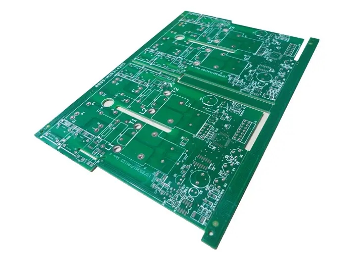
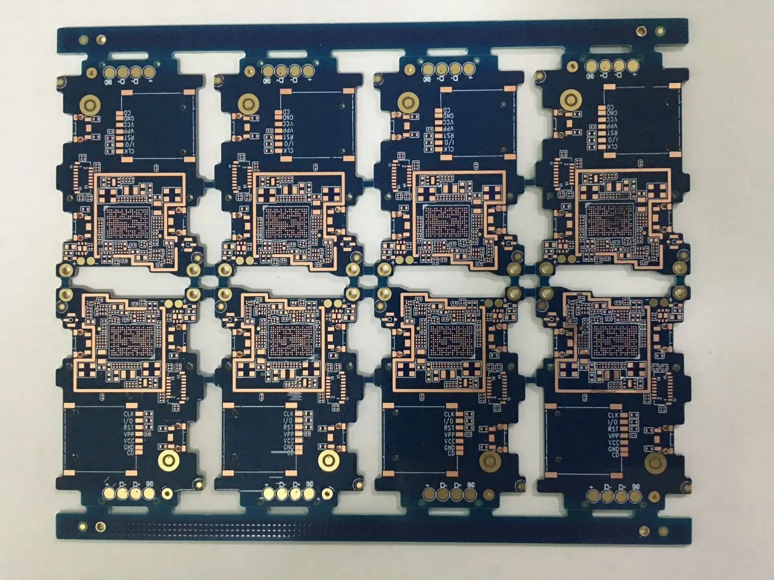
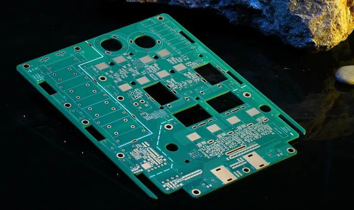
Printed circuit board (PCB) is the supporting part of circuit components and devices in electronic products. It provides the electrical connection between circuit components and devices. With the rapid development of electrical technology, the density of PGB is getting higher and higher. The anti-interference ability of PCB design has a great impact. Therefore, the general principles of PCB design and the requirements of anti-interference design must be followed when designing PCB. PCB processing, PCB assembly, PCB design, PCBA processing manufacturers will explain to you the experience summary of anti-interference design of circuit board design.


Just upload Gerber files, BOM files and design files, and the KINGFORD team will provide a complete quotation within 24h.