
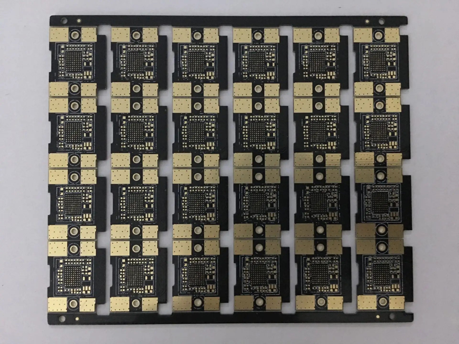
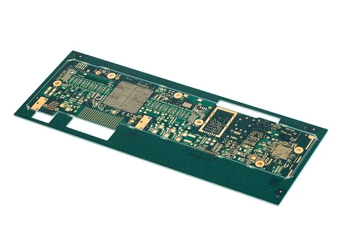
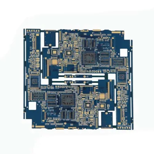
Professional PCB manufacturing and assembly
Building 6, Zone 3, Yuekang Road,Bao'an District, Shenzhen, China
+86-13410863085Mon.-Sat.08:00-20:00

Intermediate PCB Engineer of PCB Design Ability of PCB Design Engineering
Intermediate PCB Engineer
According to individual specific ability, it can be divided into three levels: A, B and C. A is the highest, followed by B
Capability requirements:
Be able to fully understand various original device manuals and wiring manuals, independently make extremely complex packages, such as placing switches, and ensure that various capabilities are completely correct (at least ensure insertion according to physical measurement), and be able to find appropriate devices or replacements according to principles and structural requirements;
Master the operation and skills of at least one PCB design software and be able to formulate detailed wiring rules;
Be able to put forward opinions on the division and integration of various functional blocks according to the system requirements, be able to reasonably arrange and route all functional blocks independently or according to the division of labor for PCB of any number of components and networks, and be able to consider the requirements of thermal design, structural design, SI, PI, EMC, aesthetics, manufacturability and other aspects at any time during the layout and routing process and propose solutions, Be able to provide some requirements and rule references in layout and wiring for entry-level and junior PCB engineers;
Be able to correctly design the laminated structure of the board, and reduce the number of layers and cost as much as possible while meeting the performance requirements;
Have more knowledge of high-speed and analog PCB design in terms of impedance, time delay, overshoot, crosstalk, loop, signal loop, plane integrity, inner layer division slot, signal termination, etc., be able to complete SI simulation and analysis of key signals and areas independently or under the guidance of SI engineers, etc., and put forward suggestions for improvement;
Be able to skillfully route and modify manually or automatically driven by rules. The whole board has a certain aesthetic feeling. More than 80% of low-level errors in the principle design can be seen and put forward during the routing process. Be able to skillfully and correctly exchange pins and gates;
Excellent communication with the principle and structure design engineers, understanding more complex mechanical drawings, and putting forward some reasonable improvement suggestions related to the principle, device selection and structure of PCB design to help the system design succeed at an early date;
The test points and silk screen marks are clear, error free, rarely make low-level errors in PCB design, and generally do not cause revision due to PCB design errors. More than 9)% of PCB processing factory projects can always be solved by feedback;
Have more knowledge of manufacturability and practice with days. More than 70% of the boards designed can be used for direct mass production.
job content:
Design and modification of extremely complex PCB (such as 8-way DVR backplane, PC motherboard, etc.);
Debugging related to self-designed PCB and SI simulation of designated parts;
Provide work instructions and wiring rules for all lower level PCB engineers;
Write relevant development and debugging logs;
Production and maintenance of internal PCB standard packaging library and standard wiring module;
If necessary, he also works as a PCB engineer of any lower level.
operating duty:
Responsible for the design part of PCB;
Responsible for the in-house PCB standard packaging library and the self-designed part of the standard wiring module;
Be responsible for their own SI simulation results and solutions. The intermediate PCB engineer, who is responsible for PCB assembly, PCB design, and PCB processing manufacturer's explanation of PCB design, is capable of PCB design engineering.


Just upload Gerber files, BOM files and design files, and the KINGFORD team will provide a complete quotation within 24h.