
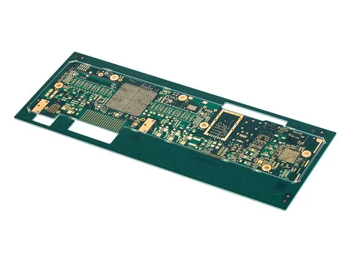
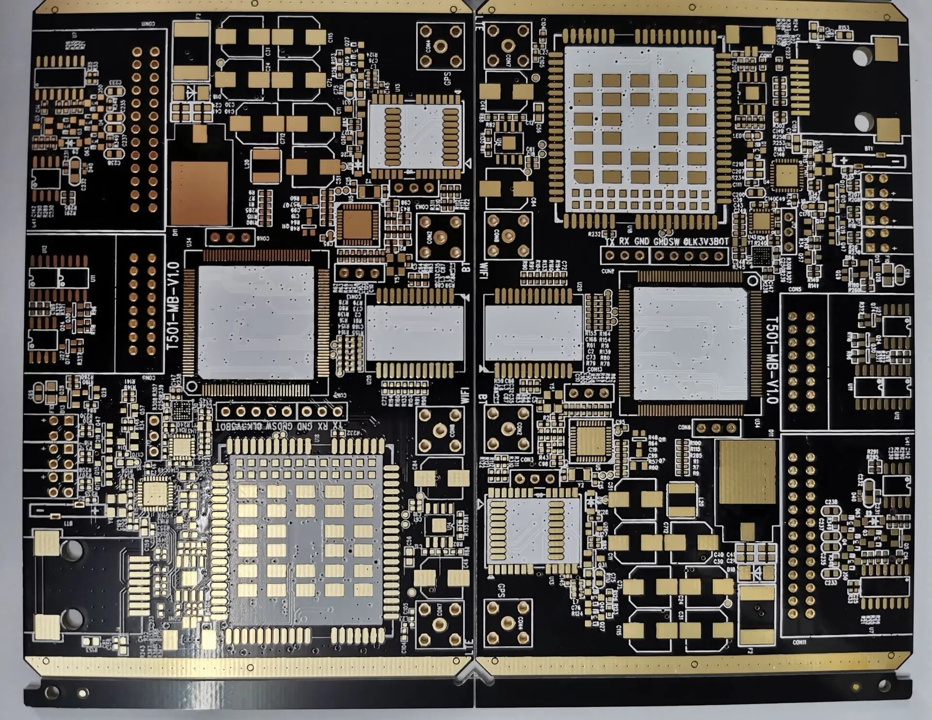
Professional PCB manufacturing and assembly
Building 6, Zone 3, Yuekang Road,Bao'an District, Shenzhen, China
+86-13410863085Mon.-Sat.08:00-20:00

People level of pcb design and primary pcb design engineering ability
Capability requirements:
Can make simple packages, such as DIP10, etc;
Master the basic operation of at least one PCB design software, and be able to formulate simple rules such as wiring line width and spacing;
It is able to carry out more reasonable and orderly layout and wiring for PCB with 100 components and 200 networks or less;
It can be manually or automatically wired and modified under other people's or self defined rules to achieve 100% routing and DRC pass completely;
Basic knowledge of mechanical structure and thermal design;
Master some basic requirements for double-sided board wiring.
job content:
Design and modification of simple PCB (such as front panel with simple structure, small system board of single chip microcomputer, etc.);
Wiring of specified parts in complex PCB;
Debugging related to self-designed PCB;
Write relevant development and debugging logs.
operating duty:
Responsible for the design part of PCB.
Junior PCB Engineer
Capability requirements:
Be able to make complex packages, such as RJ-45 seats with lights, according to the manual and physical objects, and ensure that the shape, pad and other dimensions are completely correct (at least it can be inserted according to physical objects);
Be familiar with at least one PCB design software and be able to formulate detailed wiring rules independently or under guidance;
Be able to carry out reasonable and orderly layout and wiring of single, double and multi-layer PCBs with 400 components and 1000 networks or less, and take into account the requirements of thermal design, structural design, electromagnetic compatibility design, aesthetics and other aspects at any time in the layout and wiring process. If you can't be sure, you can consult or discuss with a higher level PCB engineer in time;
Be able to skillfully route and modify manually or automatically under other people's or self determined rules, and achieve 100% routing and DRC pass completely. There are basically no problems such as line width bottleneck, inner layer islands, etc. During the routing process, a small number of low-level errors in principle design can be seen and raised, and the pins and doors can be exchanged correctly, and the network table and schematic diagram can be modified correctly;
Can correctly import and export mechanical drawings and basically understand the structural dimension requirements;
Be able to carry out some high-speed and analog PCB design under the rules or guidance of others and basically stable;
The silk screen mark is clear and clear, and can independently complete GERBER and other design output work and proofread;
Have basic knowledge of manufacturability and apply it to practice. More than 50% of the designed boards can be used for production.
job content:
Design and modification of more complex PCB (such as boards other than CPU boards in the scheduling machine, 16 screen splitter boards, etc.);
Wiring of specified parts in complex PCB;
Debugging related to self-designed PCB;
Work guidance for all lower level PCB engineers;
Write relevant development and debugging logs;
When necessary (it means that you do not have corresponding design tasks for a certain period of time, or the design work time of a PCB is urgent, and you must transfer or strengthen the designers, the same below), take any low-level PCB engineer's job. PCB factory: explain the pcb design ability that entry-level PCB engineers and junior PCB engineers need to master.
operating duty:
Responsible for the design part of PCB. PCB assembly, PCB design, and PCB processing manufacturers introduce people's level of pcb design and primary pcb design engineering capabilities.


Just upload Gerber files, BOM files and design files, and the KINGFORD team will provide a complete quotation within 24h.