
Professional PCB manufacturing and assembly
Building 6, Zone 3, Yuekang Road,Bao'an District, Shenzhen, China
+86-13410863085Mon.-Sat.08:00-20:00

Detailed introduction to challenges and skills of HDI circuit board cabling
PCB manufacturers, PCB designers and PCBA manufacturers explain the challenges and skills of HDI PCB wiring in detail
The design of printed circuit board is based on the circuit schematic diagram to realize the functions required by the circuit designer. The design of printed circuit board mainly refers to layout design, which needs to consider the layout of external connections. The optimal layout of internal electronic components, the optimal layout of metal wiring and through-hole, electromagnetic protection, heat dissipation and other factors. Excellent layout design can save production costs and achieve good circuit performance and heat dissipation.
What is HDI cabling
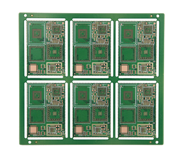
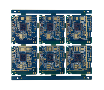
HDI (High Density Interconnects) cabling refers to the use of the latest design strategies and manufacturing technologies to achieve more intensive design without affecting circuit functions. In other words, HDI involves the use of multiple wiring layers, smaller routing, vias, pads, and thinner substrates to install complex, often high-speed circuits within a footprint that was previously impossible to achieve.
With the development of manufacturing technology, HDI cabling has begun to be seen in many designs, such as mainboards, graphics controllers, smartphones and other space constrained devices. If implemented properly, HDI cabling can not only greatly reduce the design space, but also reduce the EMI problem on PCB. Cost reduction is an important goal of the company, and HDI cabling can just achieve this.
02 HDI cabling and micro vias
It is important to understand that HDI cabling is more complex than a typical multi-layer cabling strategy. We may have designed 8-layer or 16 layer PCBs, but we still need to learn some new concepts involved in HDI wiring.
In a typical PCB design, the actual PCB is considered as a single entity and divided into multiple layers. However, HDI wiring requires design engineers to think from the perspective of integrating multiple ultra-thin layers of PCB into a single functional PCB.
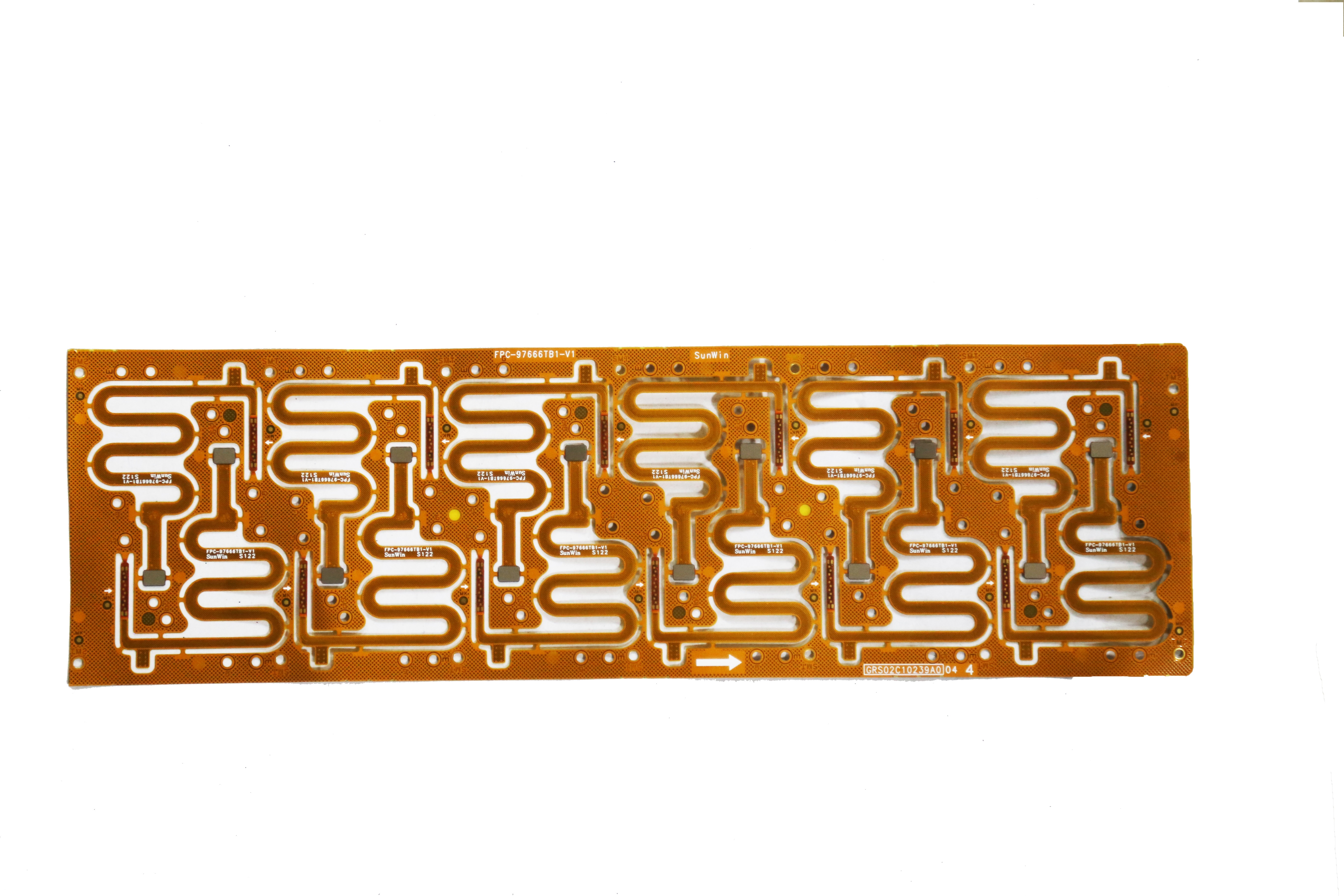
It can be said that the key driving force for HDI cabling is the development of via technology. Through holes are no longer copper plated holes drilled on each layer of PCB. The traditional via mechanism reduces the wiring area in PCB layers that are not used by signal lines.
Traditional vias have no place in HDI cabling.
In HDI cabling, micro vias are the focus of promotion and are responsible for integrating multi-layer dense cabling. For easy understanding, it can be considered that micro vias are composed of blind holes or buried holes, but have different structural methods. The traditional through hole is drilled with a drill bit after the layers are combined. However, micro vias are drilled on each layer with laser before each layer is stacked. Laser drilled micro vias allow interconnections between layers with the minimum aperture and pad size. This facilitates fan out layout of BGA components, where pins are arranged in a grid. PCB manufacturers, PCB designers and PCBA manufacturers will explain the challenges and skills of HDI PCB wiring in detail.


Just upload Gerber files, BOM files and design files, and the KINGFORD team will provide a complete quotation within 24h.