
Professional PCB manufacturing and assembly
Building 6, Zone 3, Yuekang Road,Bao'an District, Shenzhen, China
+86-13410863085Mon.-Sat.08:00-20:00

Analysis of PCB board deformation and improvement measures
What time? PCB reflow soldering, most of them are prone to bending and deformation In serious cases, it may even cause the component to become empty How to overcome it?
1. This hazards of circuit board deformation
In the automated surface mount line, if the circuit board is not flat, it cannot insert or delete components, even Circuit board, and The Board of Directors cannot Therefore, the assembly plant encountered warping of the circuit board. This is very annoying The current SMT technology is moving towards high speed and intelligence, which puts forward higher requirements In IPC standards, it is specifically pointed out that: 75%, and the allowable deformation of concrete is. 5% for PCB without surface mounting In order to meet the requirements of high precision and reliability, some electronic assembly manufacturers have stricter requirements The PCB is made of, resin, glass cloth and other materials Body By, thermal stress is inevitable, which will lead to At the same time, in the PCB processing process, it, mechanical cutting, wet treatment, etc. Various processes will also have an important impact on the environment In short, the causes of deformation PCB board they are complex and diverse How to reduce or eliminate PCB manufacturers
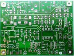
PCB board
2. Analysis of the causes of deformation
The deformation of PCB needs to be studied from several aspects such as data, structure, mode distribution, processing, etc This paper will analyze and explain the possible causes of deformation and the improvement methods Uneven copper surface area on the circuit board will aggravate the bending and warping of the circuit board In general, a large area of copper foil is designed on the circuit board for grounding. Sometimes the Vcc layer is very thin, while the other layer is a large area of copper foil When these large area copper foils are unevenly distributed on the same circuit board, it will lead to uneven heat absorption and heat dissipation Of course, the circuit board will also expand Cold shrink If expansion and contraction cannot be carried out at the same time, it will cause different stresses and deformations At this time, if the temperature of the circuit board has reached the upper limit of Tg value, the board of directors will open It begins to soften, causing deformation The connection points (vias, vias) of each layer on the circuit board will limit the expansion and contraction of the board. Today's circuit boards are mostly multilayer boards, and there are connection points (vias) like drives between the layers. The connection points are again divided into through holes, blind holes and buried holes. Where there are connection points, the influence of expansion and contraction of the board will be limited, which will also indirectly lead to bending and warping of the circuit board The weight of the board will cause it to sag and deform In general, the reflow furnace will use a chain to drive the circuit board forward in the reflow furnace, that is, both sides of the board are used as fulcrums to support the whole board If there are heavy objects on the board, or if the circuit board is too large, due to the number of the circuit board itself, it will show a depression in the middle, causing the circuit board to bend The depth of the V-cut is basically the same as the video of the connecting strip. V-Cut is the culprit that destroys the structure of the board of directors Because the V-shaped notch cuts the groove on the original large plate, the position of the V-shaped notch is easy to deform
2.1 Data impact analysis, structure, and graphics on the deformation of the plate
The PCB board is formed by pressing core board, prepreg and external copper foil The core plate and copper foil are deformed when pressed The amount of deformation depends on the coefficient of thermal expansion (CTE) of the two materials The coefficient of thermal expansion of the copper foil (CTE) is left and right, while the common FR-4 substitute is at the Z-direction CTE below the Tg point; Above the TG point is (250~350) X10-6. CTE in X direction is similar to copper foil due to the existence of glass cloth Note on TG point: when the temperature of high TG printed board rises to a certain area, the substrate will change from "glass like" to "rubber like", and the temperature at this time is called the glass transition temperature (Tg) of the board That is, Tg is the temperature (° C) at which the base material maintains rigidity In other words, the substrate of ordinary PCB will not only soften, deform, melt, etc, At high temperatures At the same time, it also shows a sharp decline in mechanical and electrical characteristics In general, the Tg of the plate exceeds 130 degrees, the high Tg is usually greater than 170 degrees, and the medium Tg is about 150 degrees Generally, PCB printed boards with a Tg of 170 ° C are called high Tg printed boards With the addition of Tg to the substrate, the heat resistance, moisture resistance, chemical resistance, PCB stability and other characteristics will be continuously improved The higher the TG value, the better the temperature resistance of the circuit board, especially in lead-free process, where high Tg applications are more common High Tg refers to high heat resistance With the rapid development of the electronic industry, especially the electronic products represented by computers, the development of high functionality and high multilayer films puts forward higher requirements for the heat resistance of materials. PCB substrate is an important guarantee The emergence and development of representative high-density installation technology have made great achievements PCB s more and more acceptable from the support of the high heat resistance of the
Subtract in terms of small aperture, fine wiring, and thinning Therefore, the difference between ordinary FR-4 and high Tg FR-4 lies in the mechanical strength, dimensional stability, adhesion, water absorption, and thermal decomposition of data under thermal state, especially when heating after moisture absorption In various cases, such as expansion, there are differences High Tg products are obviously superior to PCB substrates of ordinary products Due to the difference between pattern distribution and core plate thickness or data characteristics, the core plate with inner layer pattern has different expansion When the pattern distribution is different from the core plate thickness or data characteristics, it will be different When the pattern distribution is relatively uniform, the material type is the same It will deform Asymmetrical or uneven PCB laminate structure will lead to large difference in thermal expansion coefficient of different core boards, which will lead to deformation in the process of lamination The deformation mechanism can be explained by the following principles Suppose that two core plates with different CTEs are pressed together by prepreg, of which core plate A has CTE of 1.5x10⁻⁵/℃ and core plate length of 1000mm The pressing process is used as a prepreg for adhesive sheets, where two core plates are bonded together through three softening stages, flowing and filling with patterns, and curing At this time, the deformation of the two core plates are strictly â ³ LA=(180 degree Celsius~30 degree Celsius) x1.5x10-5m/℃ x1000mm=2.25mm; â ³ LB=(180 degree Celsius~30 degree Celsius) X2.5X10-5M/Celsius x100mm=3.75mm In Free State, the two core plates are long and short, do not interfere with each other, and have not been deformed When pressure is applied, it will be kept at high temperature for a period of time until the semi curing is completely cured At this time, the resin becomes solidified and cannot flow freely The two core boards are combined When the temperature drops, if there is no resin bonding between layers, the core board will return to its original length without deformation The upper two core plates are bonded by curing resin at high temperature and cannot shrink at will during cooling A Core plate should shrink 3.75 mm In fact, when the shrinkage is greater than 2.25 mm, it
will be hindered by the A core board. The force between the two core plates is balanced. The B core plate cannot shrink to 3.75mm, and the A core plate shrinks more than 2.25mm, so that the whole plate faces the B core plate
Printed circuit board
2.2 Deformation caused during PCB processing
The reason for the deformation of the PCB is very complex, which can be divided into two types of stress: thermal stress and mechanical stress Among them, thermal stress is mainly generated in the pressing process, and mechanical stress is mainly generated in the stacking process, processing, and baking tray The following is a brief discussion in the order of the process Introduced copper clad plate: the copper clad plate is double-sided, symmetrical in structure and without figures The thermal expansion coefficients of copper foil and glass cloth are almost the same. In addition, the difference of CTE will hardly cause deformation during pressing However, the size of the copper clad laminate press is very large, and there is a temperature difference in different areas of the hot plate, which will lead to a slight difference in the resin curing speed and degree in different areas during the pressing process, and different temperatures will rise The dynamic viscosity at different speeds also varies greatly. In addition, due to the differences in the curing process, local stresses may also occur Generally, this pressure will keep balance after pressing, but will gradually release and deform in the future processing
Pressure: Pressure PCB stamping process is the main process of generating thermal stress The deformation caused by different data or structures is shown in the analysis in the previous section Similar to the pressing of CCL, the difference in curing process will also cause local stress Due to the thicker thickness of PCB, the thermal stress of S is larger than that of CCL, with diversified pattern distribution and more prepreg The pressure PCB in life is released, shaped, or barbecued during the subsequent drilling process, resulting in deformation of the PCB
Baking process of welding mask, characters, etc.: Because solder resist inks cannot be stacked with each other during curing, PCB board will place them on the shelf for curing The welding mask temperature is about 150 ℃, just exceeding the Tg point of medium and low Tg data The resin above Tg point has high elasticity, and the plate is easy to deform under its own weight or strong wind in the oven
Hot air solder leveling: the temperature of tin furnace is 225 ℃~265 ℃, and the leveling time of hot air solder for ordinary plate is 3S-6S The temperature of hot air is between 280 ℃ and 300 ℃ After the solder is leveled, the plate enters the tin furnace from room temperature, and the post-treatment water washing at room temperature will be carried out within two minutes after the furnace is out The whole hot air solder leveling process is a sudden heating and cooling process
Due to the different data of the circuit board, the structure is uneven In this process, thermal stress will inevitably occur, resulting in micro strain and overall deformation warping zone
Storage: The packaging for storing semi-finished PCB boards is usually firmly inserted on the shelf, and the tightness of the shelf is not adjusted properly, or the stacking of boards during storage may cause mechanical deformation of the boards Especially for thin plates below 2 0mm, the impact is more serious In addition to the above factors, there are many factors that will affect PCB


Just upload Gerber files, BOM files and design files, and the KINGFORD team will provide a complete quotation within 24h.