
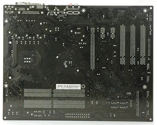
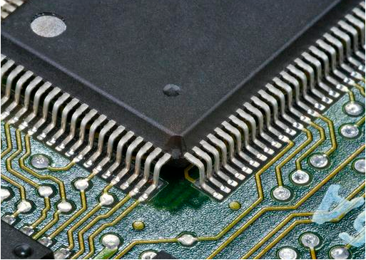
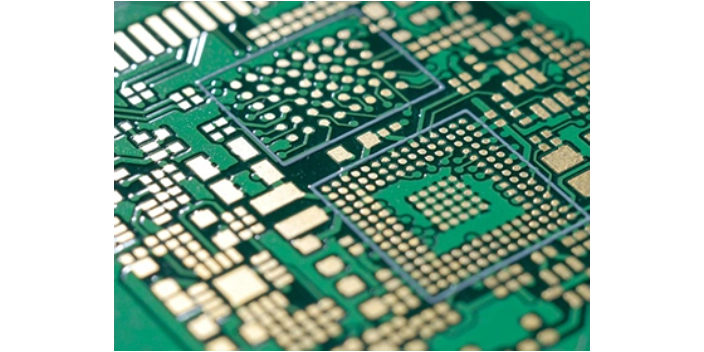
Professional PCB manufacturing and assembly
Building 6, Zone 3, Yuekang Road,Bao'an District, Shenzhen, China
+86-13410863085Mon.-Sat.08:00-20:00

Cadence: board level PCB design software and circuit system
Cadence is a large EDA software, which can complete almost all aspects of electronic design, including ASIC design, FPGA design and PCB design. Cadence has absolute advantages in simulation, PCB design, automatic layout and routing, layout design and verification. Cadence contains many tools, almost including all aspects of EDA design. The following mainly introduces its board level circuit design system.
The board level circuit design system includes schematic diagram input, generation, analog digital/hybrid circuit simulation, FPGA design, PCB editing and automatic layout MCM circuit design, high-speed PCB layout design simulation, etc.
These include:
A. Concept HDL (schematic design input tool)
Concept HDL schematic design input tool is the schematic design input system of Cadence Company. It provides users with a comprehensive, efficient and flexible schematic design environment, with powerful operation and editing functions. The designer can complete the whole schematic design process in HDL environment, and can input hierarchical schematic and planar schematic, check schematic, generate bill of materials, generate net list, etc. HDL can also be well integrated with Allegro tools in a project, which can facilitate interactive operations such as importing schematic diagrams to PCB, and reverse labeling PCB changes to schematic diagrams.
B. Check Plus HDL
Check Plus HDL schematic design rule checking tool is Cadence's schematic design rule checking standard. You can highlight all non-standard parts in PCB design schematic diagram and give reasons for them.
C. Allegro Expert
Allegro has a complete set of constraints. Users only need to set the routing rules as required to meet the design requirements of routing without violating the DRC during routing, thus saving tedious manual inspection time and improving work efficiency! It can also define parameters such as minimum line width or line length to meet the various requirements of high-speed circuit board cabling today.
D. SPECTRA Expert AutoRouter
Automatic routing means that after setting the constraints and applying the rules created, the automatic routing will achieve similar results as expected. Of course, some sorting work may also be required, and the space for other signal and network routing needs to be ensured. After part of the design is completed, fix it to prevent it from being affected by the later wiring process.
E. SigNoise (signal noise analysis tool)
Signal to noise ratio is the ratio of signal voltage to noise voltage, usually expressed by the symbol s/n. In general, the signal voltage is much higher than the noise voltage, and the ratio is very large. The unit of the signal to noise ratio is db. SigNoise analysis tool is used to analyze the cause of SNR in the circuit.
F. EMControl
Electromagnetic compatibility (EMC) refers to the ability of equipment or system to operate in accordance with requirements in its electromagnetic environment without generating unbearable electromagnetic interference to any equipment in its environment. Therefore, EMC includes two requirements: on the one hand, the electromagnetic interference generated by the equipment to the environment during normal operation cannot exceed a certain limit; On the other hand, it means that the appliance has a certain degree of immunity to electromagnetic interference existing in the environment, that is, electromagnetic sensitivity. EMControl is an electromagnetic compatibility checking tool prepared for circuit design.
G. Synplify FPGA/CPLD (integrated tool)
Synplify Pro is a high-performance FPGA integrated tool, which provides an excellent HDL integrated solution for complex programmable logic design. It includes the BEST algorithm to optimize the overall design; Automatically Retiming the critical path can improve the performance by up to 25%; Support mixed design input of VHDL and Verilog, and support netlist * Edn file input; Enhanced support for System Verilog; The pipeline function improves the performance of the multiplier and ROM; The finite state machine optimizer can automatically find the optimal coding method; Interactively index the timing report, RTL view and RTL source code; Automatic identification of RAM avoids complicated RAM instantiation.
H. Advanced Package Designer
Characteristics of MCM-D There are two hot topics in the field of microelectronic packaging today, one is BGA, the other is MCM. BGA was originally developed as a monolithic package with extremely high package density, which reduced the size of monolithic circuits.


Just upload Gerber files, BOM files and design files, and the KINGFORD team will provide a complete quotation within 24h.