
Professional PCB manufacturing and assembly
Building 6, Zone 3, Yuekang Road,Bao'an District, Shenzhen, China
+86-13410863085Mon.-Sat.08:00-20:00

A good PCB layout design can optimize the efficiency, reduce the thermal stress, and minimize the noise and effect between the wiring and components. All this comes from the designer's understanding of the current conduction path and signal flow in the power supply.
When a prototype power board is powered up for the first time, the best case is that it can not only work, but also be quiet and low in heat. However, this situation is rare.
A common problem with switching power supplies is the "unstable" switching waveform. Sometimes, the waveform jitter is in the sound band, and the magnetic components will produce audio noise. If the problem is in the layout of the printed circuit board, it may be difficult to find the cause. Therefore, the correct PCB layout at the initial stage of switching power supply design is critical.
The power designer should have a good understanding of the technical details and the functional requirements of the final product. Therefore, from the beginning of the PCB design project, the power designer should work closely with PCB layout designers on key power layout.
A good layout design can optimize power efficiency and reduce thermal stress; More importantly, it minimizes the noise and the interaction between wiring and components. To achieve these goals, designers must understand the current conduction path and signal flow inside the switching power supply. In order to achieve the correct layout design of the non disconnector power supply, it is important to keep the following design elements in mind.
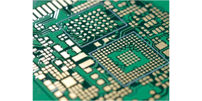
PCB design layout
PCB layout planning
For the embedded dc/dc power supply on a large circuit board, in order to obtain the best voltage regulation, load transient response and system efficiency, it is necessary to make the power output close to the load device, and minimize the interconnection impedance and conductive voltage drop of PCB wiring. Ensure good air flow and limit thermal stress; If forced air cooling measures can be adopted, the power supply shall be close to the fan.
In addition, large passive components (such as inductors and electrolytic capacitors) shall not block the airflow through low surface mounted semiconductor components, such as power MOSFETs or PWM controllers. In order to prevent switching noise from interfering with analog signals in the system, it is necessary to avoid laying sensitive signal lines under the power supply as far as possible; Otherwise, an internal ground plane needs to be placed between the power layer and the small signal layer for shielding.
The key is to plan the location of power supply and the demand for space at the early design and planning stage of the system. Sometimes designers ignore this advice and focus on the more "important" or "exciting" circuits on large system boards. Power management is regarded as an afterthought, and the power supply is placed on the spare space on the circuit board casually, which is very unfavorable to the efficient and reliable power supply design.
For multilayer boards, a good method is to lay a DC ground or DC input/output voltage layer between the high current power element layer and the sensitive small signal routing layer. The stratum or DC voltage layer provides AC ground for shielding small signal wiring, so that it is free from interference of high noise power wiring and power components.
As a general rule, neither the grounding layer nor the DC voltage layer of the multilayer PCB should be separated. If such separation is unavoidable, the number and length of wires on these layers shall be reduced as far as possible, and the laying of wires shall keep the same direction with the large current to minimize the impact.
Power stage layout
The switching power supply circuit can be divided into power stage circuit and small signal control circuit. The power stage circuit contains components used to transmit large current. Generally, these components should be laid first, and then small signal control circuits should be laid at some specific points of the layout.
The high current wiring shall be short and wide to minimize the inductance, resistance and voltage drop of PCB. This is particularly important for those lines with high di/dt pulse current.
High frequency decoupling capacitance CHF should be 0.1 μ F~10 μ F. Ceramic capacitor of X5R or X7R dielectric, which has extremely low ESL (effective series inductance) and ESR (equivalent series resistance). Larger capacitive dielectrics (such as Y5V) may reduce the capacitance value greatly under different voltages and temperatures, so they are not the best material for CHF.
If there is no heat sink for surface mounted power MOSFETs and inductors in the PCB design, the copper foil area must have sufficient heat dissipation area. For DC voltage nodes (such as input/output voltage and power supply ground), the reasonable method is to make the copper foil area as large as possible.
More vias help to further reduce thermal stress. To determine the appropriate copper foil area of high dv/dt switch nodes, a design balance should be made between minimizing dv/dt related noise and providing good MOSFET heat dissipation.
Power pad type
Pay attention to the pad form of power components, such as low ESR capacitor, MOSFET, diode and inductor.
For decoupling capacitors, the positive and negative vias should be as close to each other as possible to reduce the ESL of PCB. This is particularly effective for low ESL capacitors. Capacitors with small capacitance and low ESR are usually expensive. Incorrect pad form and poor wiring will reduce their performance, thus increasing the overall cost. In general, a reasonable pad form can reduce PCB noise, reduce thermal resistance, and minimize wiring impedance and voltage drop of high current PCB components.
A common mistake in the layout of high current power components is the incorrect use of thermal relief. If the hot air pad is used unnecessarily, the interconnection impedance between power components will be increased, resulting in greater power loss and reducing the decoupling effect of small ESR capacitors. If vias are used to conduct large currents during layout, ensure that they are sufficient to reduce impedance. In addition, do not use hot air pads for these vias.
Control circuit layout
Keep the control circuit away from the high noise switch copper foil area. For the step-down converter, a good way is to place the control circuit close to the VOUT+terminal, while for the step-up converter, the control circuit should be close to the VIN+terminal, so that the power wiring can carry continuous current.
If space allows, there should be a small distance (0.5 inch~1 inch) between the control IC and the power MOSFET and inductor (they are high noise and high heat elements). If the space is tight and the controller is forced to be placed close to the power MOSFET and inductor, special attention shall be paid to the ground or ground wiring to isolate the control circuit from the power element.
The control PCB circuit shall have an independent signal (analog) ground different from the power level ground. If there are independent SGND (signal ground) and PGND (power ground) pins on the controller IC, they should be wired separately. For the control IC integrated with MOSFET driver, the IC pin of small signal part shall use SGND.
Only one connection point is required between signal ground and power ground. The reasonable method is to return the signal to a clean point of the power formation. Only connect two kinds of grounding wires under the controller IC to realize two kinds of grounding.
The decoupling capacitors of the control IC should be close to their respective pins. To minimize the connection impedance, a good way is to connect the decoupling capacitor directly to the pin without passing through the via.
Loop area and crosstalk
Two or more adjacent conductors may produce capacitive coupling. The high dv/dt on one conductor will couple the current on the other conductor through the parasitic capacitance. In order to reduce the coupling noise of the power level to the control circuit, the high noise switch wiring should be far away from the sensitive small signal wiring. If possible, high noise routing and sensitive routing shall be laid on different layers, and internal layers shall be used as noise shielding.
If space allows, the control IC should be a small distance (0.5 in.~1 in.) from the power MOSFET and the inductor, which have both large noise and heat.
The FET driver TG, BG, SW and BOOST pins on the LTC3855 controller have high dv/dt switching voltage. The LTC3855 pins connected to the most sensitive small signal node are: Sense+/Sense -, FB, ITH and SGND. If the sensitive signal routing is close to the high dv/dt node during the layout, the ground wire or ground plane must be inserted between the signal routing and the high dv/dt routing to shield the noise.
When laying out the gate drive signal, it is helpful to minimize the impedance in the gate drive path by using short and wide routing.
If a PGND layer is laid under the BG routing, the AC ground return current of low FET will be automatically coupled to a path close to the BG routing. The AC current will flow to the smallest loop/impedance it finds. At this time, the low gate driver does not need an independent PGND return routing. The best way is to minimize the number of layers through which the grid drive wiring passes, so as to prevent grid noise from spreading to other layers.
Among all small signal routing, current detection routing is most sensitive to noise. The amplitude of current detection signal is usually less than 100mV, which is equivalent to the amplitude of noise. Taking LTC3855 as an example, Sense+/Sense routing should be arranged in parallel with minimum spacing (Kelvin detection) to minimize the chance of picking up di/dt related noise.
In addition, the filter resistance and capacitance of the current detection wiring should be as close to the IC pin as possible. This structure has the best filtering effect when there is noise injection into the long detection line. If inductance DCR current detection with R/C network is adopted, DCR detection resistance R shall be close to inductance, and DCR detection capacitance C shall be close to IC
If a via is used on the return path from the routing to Sense -, the via should not contact other internal VOUT+layers. Otherwise, the via may conduct large VOUT+current, and the voltage drop generated may destroy the current detection signal. Avoid laying current detection lines near high noise switch nodes (TG, BG, SW and BOOST lines). If possible, place a layer between the layer where the current detection wiring is located and the power level wiring layer.
If the controller IC has differential voltage remote detection pin, independent wiring shall be used for positive and negative remote detection lines, and Kelvin detection connection shall also be used.
Selection of wiring width
For specific PCB controller pins, the current level and noise sensitivity are unique, so you must select a specific wiring width for different signals. Generally, the small signal network can be narrower, and the routing width of 10mil~15mil is adopted; High current network (grid drive, VCC and PGND) shall adopt short and wide routing.
Interpret PCB design high current path setting
Nov 01,2022


Just upload Gerber files, BOM files and design files, and the KINGFORD team will provide a complete quotation within 24h.