
Professional PCB manufacturing and assembly
Building 6, Zone 3, Yuekang Road,Bao'an District, Shenzhen, China
+86-13410863085Mon.-Sat.08:00-20:00

Common splicing methods of PCBA circuit board
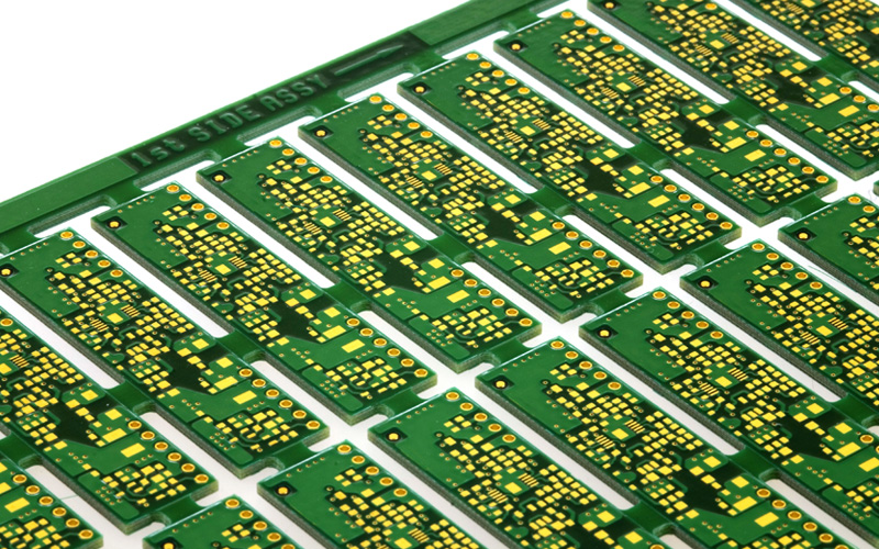
The pcb splicing is just for the convenience of production. For the plate factory, its base material is generally large. It makes many boards at a time, and then cuts them one by one. If the splicing is mainly used in welding production, imagine that a board with a large nail cover is welded one by one on a SMT machine as big as a car.
Pcb panel has several definitions! Convenience plug-in is a convenience for manufacturers to produce is a material saving is a! Convenient plug-in is the combination of customer requirements, and you must do it according to requirements. The manufacturer is convenient for production, such as V cutting. Material saving is to use materials more perfectly without wasting or leaving too much leftovers!
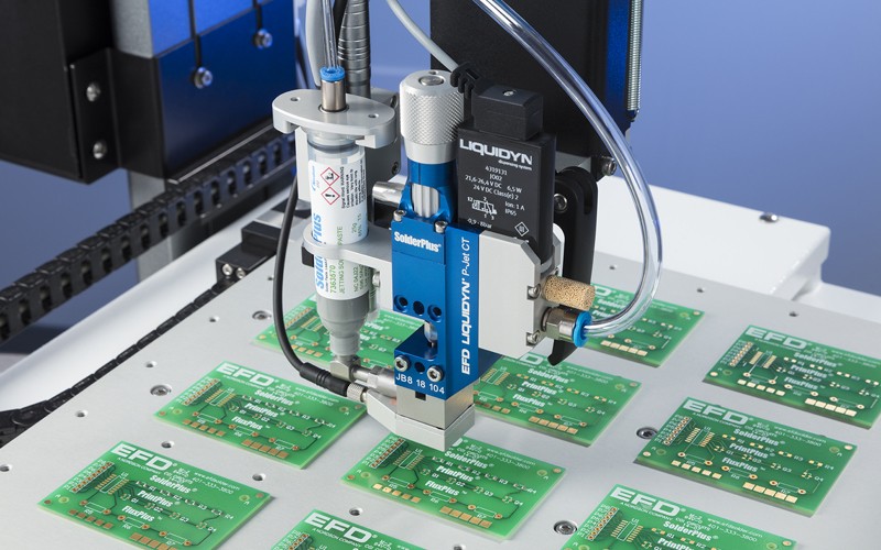
In order to improve production efficiency and reduce production costs during PCBA processing, PCBA circuit boards are usually assembled for production, which can facilitate PCBA processing plants to carry out patch welding. Now let's talk about the common methods and principles of PCBA circuit board.
Principles of PCBA circuit board assembly:
1. PCB panel width ≤ 260mm (SIEMENS line) or ≤ 300mm (FUJI line); If automatic dispensing is required, PCB panel width × Length ≤ 125mm × 180mm。
2. PCB panel shape should be as close to square as possible, and 2 is recommended × 2、3 × 3、4 × Grade 4 panel; But be careful not to make up the yin and yang plates.
3. The outer frame (clamping edge) of the PCB panel shall adopt a closed loop design to ensure that the PCB panel will not deform after being fixed on the fixture.
4. The center distance between small plates shall be controlled between 75mm and 145mm.
5. There shall be no large components or protruding components near the connection point between the outer frame of the panel and the internal small board, or between the small board and the small board, and a space of more than 0.5mm shall be reserved at the edge of the components and PCB board to ensure the normal operation of the cutting tool.
6. Make four positioning holes at the four corners of the outer frame of the panel, with the hole diameter of 4mm ± 0.01mm; The strength of the hole shall be moderate to ensure that it will not break during the process of upper and lower plates; The hole diameter and position accuracy shall be high, and the hole wall shall be smooth without burrs.
7. Each small board in the PCB assembly must have at least three positioning holes, 3 ≤ aperture ≤ 6mm, and no wiring or patch is allowed within 1mm of the edge positioning hole.
8. In principle, QFP with spacing less than 0.65mm shall be set at its diagonal position for the reference mark used for PCB whole board positioning and fine pitch device positioning; The positioning datum symbols used for the sub boards of the assembled PCB shall be used in pairs and arranged at the opposite corners of the positioning elements.
9. When setting the datum locating point, a non blocking area 1.5mm larger than the locating point is usually reserved around the locating point.
10. Large components shall be provided with positioning posts or holes, especially I/O interfaces, microphones, battery interfaces, microswitches, headphone interfaces, motors, etc.
Common assembly methods of PCBA circuit board:
1、V-CUT
V-CUT means that several boards or the same boards can be combined and spliced together, and then a V-CUT machine can be used to cut a V-shaped slot between boards after PCB processing is completed, which can be broken during use. It is a popular way nowadays.
2. Flume
Punching groove refers to milling between circuit boards or inside boards with milling machine as required, which is equivalent to digging out.
3. Stamp hole
The so-called stamp use refers to the use of very small holes to link the plates, which looks like the sawtooth shape on the stamps, so it is called stamp hole link. Stamp hole link requires high burr control around the board, that is, only a few stamp holes can be used to replace the V line.


Just upload Gerber files, BOM files and design files, and the KINGFORD team will provide a complete quotation within 24h.