
Professional PCB manufacturing and assembly
Building 6, Zone 3, Yuekang Road,Bao'an District, Shenzhen, China
+86-13410863085Mon.-Sat.08:00-20:00

Shenzhen pcb manufacturer explains the causes and control methods of tin beads in SMT production
Over the past 20 years, with the continuous development of electronic information products in light, thin, power saving, miniaturization and planarization, surface mount technology (SMT) must be used for electronic products with different purposes. However, tin beads are very harmful to electronic products, so how to reduce tin beads is one of the key control contents of SMT enterprises.
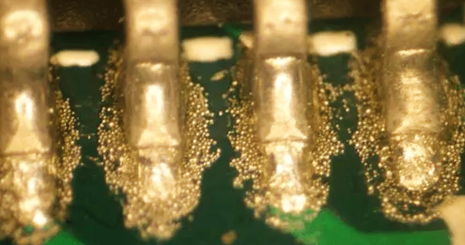
According to relevant cases, during reflow soldering in SMT production, due to the splashing of solder paste metal particles, it is easy to form small spherical solder beads or irregular solder particles, which are called solder beads. Tin bead is one of the main defects in SMT production, with a diameter of about 0.2~0.4mm. It mainly appears on the side of SMT components or between IC pins. It not only affects the appearance of PCB products, but also may cause short circuit in use, seriously affect the quality and life of electronic products, and even cause personal injury.
Tin bead is caused by many factors, such as raw materials, solder paste, steel mesh, mounting, reflow soldering, and environment. Therefore, it is very important to study the causes of it and strive for the most effective control.
Tin bead produced due to raw material problem and its control method
1. PCB quality and components
The PCB pad (PAD) design is unreasonable. If the component body presses too much on the PAD and extrudes too much solder paste, solder beads may be generated.
When designing PCB, it is necessary to select appropriate component packaging and appropriate PAD.
PCB solder mask has poor printing and rough surface, resulting in tin beads during reflow. Incoming PCB material inspection must be tightened. If the solder mask is seriously defective, it must be returned or scrapped.
If solder beads are produced due to moisture or dirt on the bonding pad, the moisture or dirt on the PCB must be carefully removed before it is put into production.
In addition, we often encounter the substitution requirements of devices with different package sizes supplied by customers, resulting in mismatch between devices and PADs, which is easy to produce solder beads. Therefore, we should try to avoid substitution.
2. PCB is affected with moisture
There is too much water in the PCB. When the PCB passes through the reflow furnace after mounting, gas is generated due to the rapid expansion of water, resulting in tin beads. It is required that PCB must be packaged in a dry vacuum before being put into SMT production, and if it is damp, it needs to be baked in an oven before use. Baking is not allowed for organic solder mask (OSP) plates. According to the production cycle, the OSP board can be put into production within 3 months, and the OSP board needs to be replaced after 3 months.
3. Selection of solder paste
Solder paste significantly affects the welding quality. The metal content, oxide content, metal powder particle size, paste activity, etc. in the solder paste affect the formation of solder beads to varying degrees.
Metal content and viscosity. Normally, the volume ratio of the metal content in the solder paste is about 50%, the mass ratio is about 89%~91%, and the rest is flux, rheology regulator, viscosity control agent, solvent, etc. If the proportion of flux is too large, the viscosity of solder paste will be reduced. In the preheating area, too much force generated when the flux is vaporized is easy to produce solder beads. Solder paste viscosity is an important factor affecting the printing performance, usually between 0.5 and 1.2 K Pa · s. When steel screen printing, the best solder paste viscosity is about 0.8 KPa · s. When the metal content increases, the viscosity of solder paste increases, which can more effectively resist the force generated by gasification in the preheating area, reduce the slump trend of solder paste after printing, and reduce solder beads.
Oxide content. The oxide content in the solder paste also affects the welding effect. The higher the oxide content is, the greater the resistance of the metal powder in the bonding process after melting. In the reflow phase, the oxide content on the metal powder surface will also increase, which is not conducive to the "wetting" of the bonding pad and the generation of tin beads. Therefore, it is necessary to conduct true cavitation operation in the manufacturing process of metal powder (Powder) to prevent oxidation of Powder.
Particle size and uniformity of metal powder. Metal powder is a very small spherical particle. Its shape, diameter and uniformity affect its printing performance. The oxide content in the finer particles is higher. If the proportion of fine particles is large, the printing will be clearer, but the edge collapse is easy to occur, which will increase the number of tin beads; The larger the proportion of particles, the more connected tin, the greater the difference in uniformity, will lead to more tin beads.
Solder paste activity. Solder paste has poor activity and dries too fast. If excessive diluent is added, tin beads will be easily produced in the preheating area due to excessive force generated by diluent gasification. If you encounter solder paste with poor activity, you'd better stop using it immediately and replace it with one with good activity.
Tin Beads Caused by Wire Mesh Problems and Their Control Methods
If the steel mesh is too thick, the solder paste printing will be thick, and solder beads are easy to be produced after reflow soldering.
Selection principle of steel mesh thickness:
1. 0201 When the spacing between components or IC pins is ≤ 0.3mm, select 0.07-0.10mm as the thickness of the steel mesh.
2. When the spacing between 0402 components or IC pins is ≤ 0.4mm, select 0.10-0.12mm for the thickness of steel mesh.
3. 0603 When the spacing between components or IC pins is ≤ 0.5mm, select 0.12-0.15mm for the thickness of steel mesh.
If the steel mesh is too thick, resulting in too many tin beads, the steel mesh shall be remade as soon as possible.
The steel mesh opening is not provided with tin bead prevention treatment, which is easy to produce tin beads. Whether there is lead or no lead, the opening of the chip part printed with tin steel mesh shall be tin bead proof.
Improper, excessive and offset openings of the steel mesh will lead to tin beads. The PAD size determines the size of the steel mesh opening, and the most critical elements of the steel mesh opening design are size and shape. To avoid excessive solder paste printing, the opening size is designed to be less than 10% of the contact area of the corresponding pad; The lead-free steel mesh opening design should be larger than that with lead, so that the solder paste can completely cover the bonding pad as much as possible.
Tin Beads Caused by Improper Adjustment of Printer Parameter Setting and Its Control Method
After printing, the solder paste has edge collapse, which may form solder beads after passing through the reflow furnace. The solder paste has collapsed edges, which is related to the press scraper pressure, speed and demoulding speed. In case of solder paste edge collapse, it is necessary to readjust the scraper pressure, speed or demoulding speed to reduce the edge collapse and solder beads.
Printing starts when the position is not aligned. Printing is offset, which makes some solder paste stick to the PCB and may form solder beads.
Solder paste printed on PAD is too thick, and excess solder paste overflows after the component is pressed down, which is easy to form solder beads. Solder paste printing thickness is a major parameter in production, which is usually equal to (1+10% ± 15%) of the thickness of the steel mesh. If it is too thick, it is easy to form solder beads due to edge collapse.
The printing thickness is determined by the stencil thickness, which is related to the machine settings and solder paste characteristics. The micro adjustment of printing thickness is usually realized by adjusting the scraper pressure and printing speed.
Tin Beads Caused by Pressure Problem of Parts and Its Control Method
If the placement pressure in the patch is set too high, when the component is pressed on the solder paste, part of the solder paste may be squeezed under the component. In the reflow soldering stage, this part of the solder paste is easy to melt and form solder beads. Therefore, appropriate placement pressure should be selected.
Tin bead produced due to furnace temperature problem and its control method
Reflow soldering curve can be divided into four stages: preheating, heat preservation, reflow and cooling. In the preheating stage, when the temperature rises to 120~150 ℃, the volatile solvent in the solder paste can be removed and the thermal vibration to the components can be reduced; At the same time, the solder paste will be vaporized inside. If the bonding force between the metal powders in the solder paste is less than the force generated by gasification, a small amount of solder paste will overflow from the PAD, and some will hide under the sheet resistance and capacitance, forming solder beads after refluxing.
It can be seen that the higher the preheating temperature is, and the heating in the preheating zone is too fast, the more gasification splash will increase, and the easier it is to form tin beads. Therefore, adjust the temperature of the reflux furnace, reduce the speed of the conveyor belt, and adopt a moderate preheating temperature and speed to control the tin bead.
Tin bead and its control method caused by process control problems
Precautions for the use of solder paste mainly include the following aspects: under the specified storage conditions, the storage life of solder paste is generally 3-6 months;
Solder pastes shall be used according to the principle of "first in, first out", and shall be stored in a constant temperature refrigerator in a sealed form at a temperature of 2 ℃~10 ℃; Before use, take it out of the refrigerator, seal it and place it at room temperature for at least 4H. When the solder paste reaches room temperature, open the bottle cap. After taking out some solder paste, squeeze all the air between the inside cap and the solder paste, and immediately cover the outer cap. If the bottle is opened at low temperature, it is easy to absorb water vapor, and tin beads are easily produced during reflow soldering; After unsealing, stir evenly as required to reduce the viscosity of solder paste. In principle, use up the solder paste once in the same day after unsealing; When the solder paste is placed on the steel wire mesh for more than 30 minutes and is not used, it shall be mixed with the mixing function of the printing machine before use. If the interval is longer (more than 1h), the solder paste shall be put back into the tank again and the bottle cap shall be tightly covered. If it is used again, it shall be mixed evenly; When the solder paste is removed from the wire mesh, another empty can shall be used to prevent contamination of the fresh solder paste. The solder paste scraped from the wire mesh shall also be sealed and refrigerated.
The process management also has its corresponding requirements: the optimal temperature for printing is 25 ℃± 3 ℃, and the relative humidity is 45% ~ 65%. If the temperature and humidity are too high, the solder paste is easy to absorb water vapor, and the solder beads are easy to be produced when refluxing; In case of printing failure, it is better to thoroughly clean PCB with ultrasonic cleaning equipment, and then put it into the oven for baking according to specifications after drying to prevent tin beads from appearing during reuse; The steel mesh was not cleaned in time or was not wiped thoroughly, resulting in residual solder paste on the back of the steel mesh, polluting the PCB surface and producing solder beads. The operation must be carried out in strict accordance with the cleaning specifications of the steel mesh, and special personnel must be assigned to clean and inspect it; After the solder paste is printed, the PCB should be mounted in the shortest possible time to prevent solvent volatilization such as flux and easy to produce solder beads.
In SMT production, there are many factors that produce tin beads. It is not enough to focus on one aspect or adjust one parameter. We need to carefully control all details in the preparation stage before production and in the production process, and study how to control the factors that affect the solder bead, so as to achieve the best welding effect and meet the high quality requirements of the electronic connection technology.

Six Keys to Chip Manufacturing
Oct 25,2022


Just upload Gerber files, BOM files and design files, and the KINGFORD team will provide a complete quotation within 24h.