
Professional PCB manufacturing and assembly
Building 6, Zone 3, Yuekang Road,Bao'an District, Shenzhen, China
+86-13410863085Mon.-Sat.08:00-20:00

Although Protel has the function of automatic layout, but can not fully meet the needs of high-frequency circuit work, often rely on the designer's experience, according to the specific situation, first using manual layout method to optimize and adjust the position of some components, and then combined with automatic layout to complete the overall design of PCB. The reasonable layout directly affects the life of the product, stability, EMC (electromagnetic compatibility), etc., must be considered from the overall layout of the circuit board, the flexibility of the wiring and the manufacturability of the PCB, mechanical structure, heat dissipation, EMI(electromagnetic interference), reliability, signal integrity and other aspects.
Generally, the fixed position components related to the mechanical size are placed first, and then the special and larger components are placed, and finally the small components are placed. At the same time, it is necessary to take into account the requirements of wiring, the placement of high-frequency components should be as compact as possible, and the wiring of the signal line can be as short as possible, thereby reducing the cross interference of the signal line.
1.1 Placement of positioning inserts in relation to mechanical dimensions
Power outlets, switches, interfaces between PCBS, indicators, etc., are positioning plug-ins related to mechanical dimensions. Usually, the interface between the power supply and the PCB is placed on the edge of the PCB, and the PCB edge should have a spacing of 3 mm to 5 mm; Indicates that the LED should be accurately placed as needed; Switches and some fine tuning components, such as adjustable inductors, adjustable resistors, etc. should be placed near the edge of the PCB for easy adjustment and connection; Components that need to be replaced frequently must be placed in a location with fewer components for easy replacement.

1.2 Placement of special components
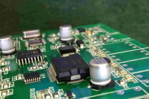
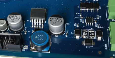
High-power tubes, transformers, rectifier and other heating devices, in the high-frequency state of the operation of the heat generated more, so in the layout should be fully considered ventilation and heat dissipation, such components placed on the PCB air easy circulation place. The high-power rectifier tube and adjusting tube should be equipped with a radiator and should be far away from the transformer. Heat-afraid components such as electrolytic capacitors should also be kept away from heat-generating devices, otherwise the electrolyte will be baked dry, causing its resistance to increase, performance to deteriorate, affecting the stability of the circuit.
Components that are prone to failure, such as adjustment tubes, electrolytic capacitors, relays, etc., should also take into account convenient maintenance when placed. For test points that often need to be measured, care should be taken to ensure that the test rod can be easily contacted when arranging components.
Because the 50 Hz leakage magnetic field is generated inside the power supply device, when it is connected to some parts of the low-frequency amplifier, it will interfere with the low-frequency amplifier. Therefore, they must be isolated or screened. It is best to arrange the amplifier at all levels in a straight line according to the schematic, and the advantage of this arrangement is that the ground current at all levels flows at this level and does not affect the work of other circuits. The input stage and the output stage should be as far away as possible to reduce the parasitic coupling interference between them.
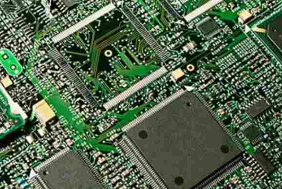
Considering the signal transmission relationship between the functional circuits of each unit, the low-frequency circuit and the high-frequency circuit should also be separated, and the analog circuit and the digital circuit should be separated. The integrated circuit should be placed in the center of the PCB, so as to facilitate the wiring connection of each pin with other devices.
Inductors, transformers and other devices have magnetic coupling, and should be placed orthogonal between each other to reduce magnetic coupling. In addition, they all have a strong magnetic field, and there should be an appropriately large space or magnetic shielding around them to reduce the impact on other circuits.
The key parts of the PCB should be configured with appropriate high-frequency decoupling capacitors, such as an electrolytic capacitor of 10μF ~ 100 μF at the input end of the PCB power supply, and a ceramic capacitor of about 0.01 pF should be connected near the power pin of the integrated circuit. Some circuits also need to be configured with appropriate high-frequency or low-frequency chokes to reduce the influence between high and low-frequency circuits. This point should be considered in the schematic design and drawing, otherwise it will also affect the performance of the circuit.
The spacing of components should be appropriate, and the spacing should take into account whether there is a possibility of breakdown or ignition between them.
For amplifiers with push-pull circuit and bridge circuit, attention should be paid to the symmetry of electrical parameters of components and the symmetry of structure when arranging, so that the distribution parameters of symmetrical components are as consistent as possible.
After the manual layout of the main components is completed, the component locking method should be used so that these components will not move during the automatic layout. Execute the Edit change command or select Locked in the Properties of the component to lock it for no further movement.


Just upload Gerber files, BOM files and design files, and the KINGFORD team will provide a complete quotation within 24h.