
Professional PCB manufacturing and assembly
Building 6, Zone 3, Yuekang Road,Bao'an District, Shenzhen, China
+86-13410863085Mon.-Sat.08:00-20:00

Use image detection on the line, and compare the pcb position.
Advanced points can also feed back position information and then adjust the component installation position. It doesn't matter if it's a little skewed.

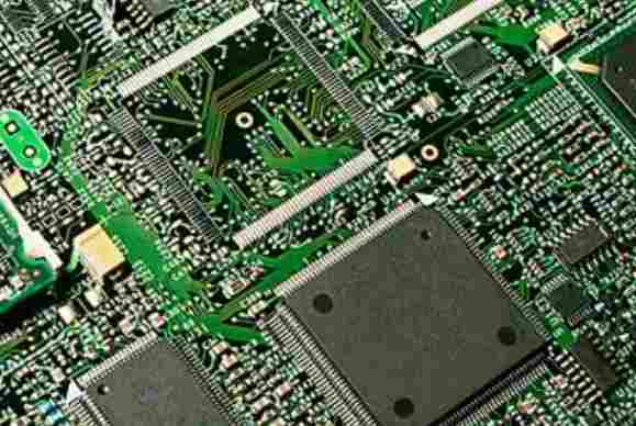
1, the role of optical image inspection system Optical image measurement system is the key equipment of modern manufacturing machinery, and is widely used in machine vision applications, such as inspection, reverse engineering and other automated industries. With the development of high-tech industry, many product testing methods in the past are now required to be tested by automated and non-contact methods. Taking the PCB industry as an example, the role of the optical image inspection system is to detect the size specification of the PCB in the manufacturing process, carry out process control, and eliminate or reduce defects by correcting the process. Usually the optical image detection system is placed in a key position to monitor the specific production situation and provide the necessary basis for the adjustment of the production process. In the PCB manufacturing process, the items to be tested: film thermal expansion and contraction detection, product appearance detection, location detection of each element, length, width and height detection, true straightness detection, roundness detection, hole burr detection, etc.
2, optical image detection system block diagram Optical image detection system is mainly composed of workbench, drive control, CCD camera system and software system 4 parts.
3, the working principle of optical image detection system Automatic optical image detection system, the core structure is a set of CCD camera system, AC servo control x, y table and image processing system. In the detection, the printed circuit board to be detected is first placed on the workbench of the optical measurement system, and after positioning, the detection program of the product to be detected is called out. The x and y workstations send the circuit board to the camera, and after the camera captures the image of the circuit board, the processor will move to the next position in the x and y workstations to capture it, and then perform the corresponding calculation.
Through the continuous processing of the image, the high detection speed is obtained. The optical image detection system automatically specifications the PCB size through the program, can input the actual value and tolerance to be measured, after analysis, processing and judgment, find defects and position prompts, while generating files, waiting for further confirmation by the operator or sent to the relevant departments for improvement.
1.3 Placement of common components
For ordinary components, such as resistors, capacitors, etc., the automatic layout can be used to consider the orderly arrangement of components, the size of the occupied space, the flexibility of wiring and the convenience of welding.
2. Wiring design
Wiring is the overall requirement of high frequency PCB design on the basis of reasonable layout. Wiring includes two ways: automatic wiring and manual wiring. Usually, regardless of the number of key signal lines, these signal lines are first routed manually, the wiring of these signal lines is carefully checked after the wiring is completed, and it is fixed after the inspection, and then other wiring is automatically routed. That is, a combination of manual and automatic wiring is used to complete PCB wiring.
Special attention should be paid to the following aspects in the wiring process of high-frequency PCB.
2.1 Direction of wiring
Circuit wiring is best in accordance with the direction of the signal to use a straight line, the need to turn the 45° line or arc curve to complete, which can reduce the high-frequency signal external transmission and mutual coupling. The wiring of high-frequency signal lines should be as short as possible. According to the working frequency of the circuit, the length of the signal line should be reasonably selected, which can reduce the distribution parameters and reduce the loss of the signal. When making a double panel, the wiring on the two adjacent levels is best perpendicular, oblique or curved to each other. Avoid parallel to each other, which reduces mutual interference and parasitic coupling.
High-frequency signal lines and low-frequency signal lines should be separated as far as possible, and shielding measures should be taken if necessary to prevent mutual interference. For the signal input that receives a relatively weak signal, it is easy to be interfered by external signals, and the ground wire can be used to shield it or do a good job of shielding the high-frequency connector. Parallel wiring should be avoided on the same level, otherwise distribution parameters will be introduced and affect the circuit. If it cannot be avoided, a grounded copper foil can be introduced between the two parallel lines to form an isolation line.
In the digital circuit, for the differential signal lines, the lines should be taken in pairs, so that they are parallel and close to each other as far as possible, and the difference is not large.
2.2 Form of wiring
In the PCB routing process, the minimum width of the line is determined by the adhesion strength between the wire and the insulating layer substrate and the strength of the current flowing through the wire. When the thickness of the copper foil is 0.05mm and the width is 1mm ~ 1.5mm, 2A current can be passed. The temperature will not be higher than 3 ° C, except for some more special wiring, the other wiring width on the same level should be as consistent as possible. The spacing of the wiring in the high frequency circuit will affect the size of the distributed capacitance and inductance, which will affect the loss of the signal, the stability of the circuit and the interference of the signal. In high speed switching circuit, the distance of the wires will affect the transmission time and the quality of the waveform. Therefore, the minimum spacing of the wiring should be greater than or equal to 0.5mm, as long as permitted,PCB wiring is best to use a relatively wide line.
There should be a certain distance between the printed wire and the edge of the PCB (not less than the board thickness), which is not only easy to install and mechanical processing, but also improves the insulation performance.
When wiring encounters a line that can only be connected around a large circle, it is necessary to use a flying line, that is, directly use a short line connection to reduce the interference caused by long-distance wiring.


Just upload Gerber files, BOM files and design files, and the KINGFORD team will provide a complete quotation within 24h.