
Professional PCB manufacturing and assembly
Building 6, Zone 3, Yuekang Road,Bao'an District, Shenzhen, China
+86-13410863085Mon.-Sat.08:00-20:00

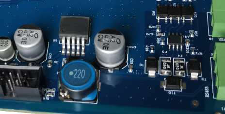
From the number of PCB layersand development direction, the PCB industry is divided into six main subdivisions, such as single panel, double panel, conventional multi-layer board, flexible board, HDI (high-density interconnection) board, packaging substrate, etc. From the four cycle dimensions of product life cycle, such as "introduction period - growth period - maturity period - recession period", single panel and double panel are in a recession period because they are not suitable for the current short and thin application trend of electronic products, and the proportion of their output value is gradually decreasing, so the number of single panel sheet and double panel sheet is also reduced. PCB board market development trend
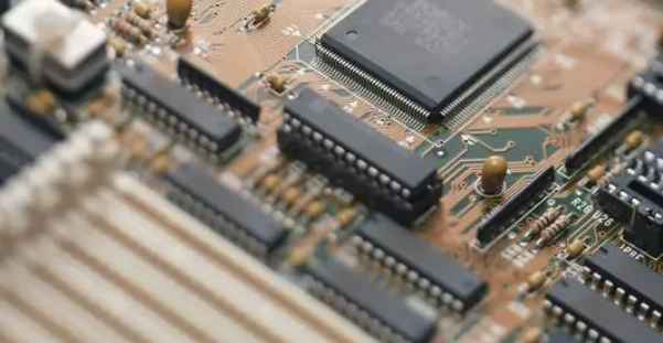
In addition, the conventional multilayer board and HDI belong to the mature stage of the product, the process capacity is increasingly mature, the product added value is high, is currently most of the main PCB factories to focus on the direction, but also PCB board companies strive to study the object. Flexible board, especially high-density flexible board and rigid combined board, due to the current technology is not mature, can not achieve a large number of manufacturers mass production, belongs to the growth period of products, but because of its characteristics more suitable for digital products than rigid board, flexible board growth is very high, is the future development direction of each large factory. PCB board companies such as Dongyuan Technology are also increasing the research and development of wound board, and have made significant progress in the field of wound board.

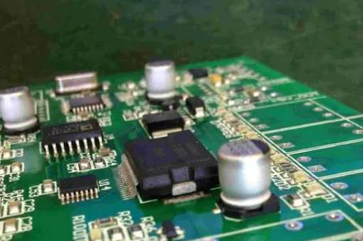
From a global point of view, PCB manufacturers are mainly distributed in China, Taiwan, Japan, South Korea, North America and Europe and other six regions. The global printed circuit board industry is relatively dispersed, with many producers and no market leader yet. As the product structure of PCB circuit boards is gradually developing to multi-layer and high-precision, PCB board companies should also adapt to The Times, vigorously carry out research in multi-layer board and high-precision board board, in order to adapt to the cloning and secondary development of high-end electronic products, master market opportunities, enhance competitiveness, and consolidate the industry position.
Ideal process - AlphaSTAR
In addition to excellent performance, an "ideal process" must also meet the safety, environmental protection and reliability requirements of the electronics industry published on July 1, 2006. Although as early as 1994, Losi Chemical has owned the patent for AlphaLEVEL product series, but Losi Chemical still continues to improve the process and research and development, and has successfully developed the third generation of silver sinking technology for printed circuit boards - AlphaSTAR. The AlphaSTAR process is specifically designed to meet today's increasingly stringent final surface treatment requirements, it addresses several of the issues discussed above that lead to board obsoletions, cost increases, environmental protection and safety, and it complies with current and future regulations that may affect the printed circuit board industry. The process has a total of 7 steps (three of which are washing steps), its performance and advantages are described as follows:
Pretreatment is divided into the following four steps: oil removal, water washing, micro-etching and water washing. The surface tension of the oil removal solution is very low, and it can wet all the copper surfaces, which eliminates the copper exposure problem and promotes the deposition of silver layers in high aspect ratio holes and micro-pores. The unique micro-etching formula can produce a slightly coarser, semi-bright surface structure, which is conducive to the formation of a silver layer with a fine and dense crystal structure, so that a high-density, low-porosity silver layer can be obtained even when the silver layer thickness is very low. This greatly improves the corrosion resistance of the silver layer.
Silver precipitation is divided into the following three steps: pre-leaching, silver precipitation and finally deionized washing. The purpose of pre-leaching is threefold: first, it is used as a sacrifice solution to prevent copper and other substances from contaminating the silver settling solution from the micro-etching tank; second, it provides a clean copper surface for the silver settling replacement reaction, so that the copper surface can obtain the same chemical environment and pH value as the silver settling solution. Since the composition of the prepreg is the same as that of the silver sink (except for metallic silver), the third function of this process is the automatic replenishment of the silver sink. The only thing consumed in the silver sedimentation reaction is metallic silver, and the change in the content of organic components in the silver sedimentation solution is only caused by the loss caused by the bath, and the preleaching and silver sedimentation solution have the same composition, and the amount brought in by the preleaching is equal to the amount brought out by the silver sedimentation solution, so the silver sedimentation solution will not accumulate unnecessary organic matter.
The silver precipitation reaction is carried out by the substitution reaction between copper and silver ions. The microcoarsened copper surface with AlphaSTAR microetching solution ensures that a uniform silver deposition layer is slowly formed at a controlled silver deposition rate. The slow precipitation rate is conducive to the deposition of a dense crystal structure, avoiding the growth of particles due to precipitation and caking, forming a high-density silver layer. This compact, moderately thick (6-12u ") silver layer not only has high corrosion resistance, but also has very good electrical conductivity. Silver sinks are very stable, have a long life cycle, and are not sensitive to light and trace halides. Other benefits of AlphaSTAR include significantly reduced downtime, low ion contamination, and low equipment costs.
V. Conclusion
The AlphaSTAR process brings together the best performance of several final surface treatments that meet and exceed the global printed circuit board industry's requirements for weldability, reliability, safety, and regulatory compliance. The AlphaSTAR process has a wide operating window; Easy to operate, control and maintain, rework operation is possible, and the production cost is the lowest in the class of final surface treatment. The AlphaSTAR process addresses the six silver-related issues discussed above, eliminating or reducing the direct impact of these issues on high-quality products. In addition, this process complies with RoHS and WEEE regulations, and the silver deposition layer is completely lead-free.


Just upload Gerber files, BOM files and design files, and the KINGFORD team will provide a complete quotation within 24h.