
Professional PCB manufacturing and assembly
Building 6, Zone 3, Yuekang Road,Bao'an District, Shenzhen, China
+86-13410863085Mon.-Sat.08:00-20:00

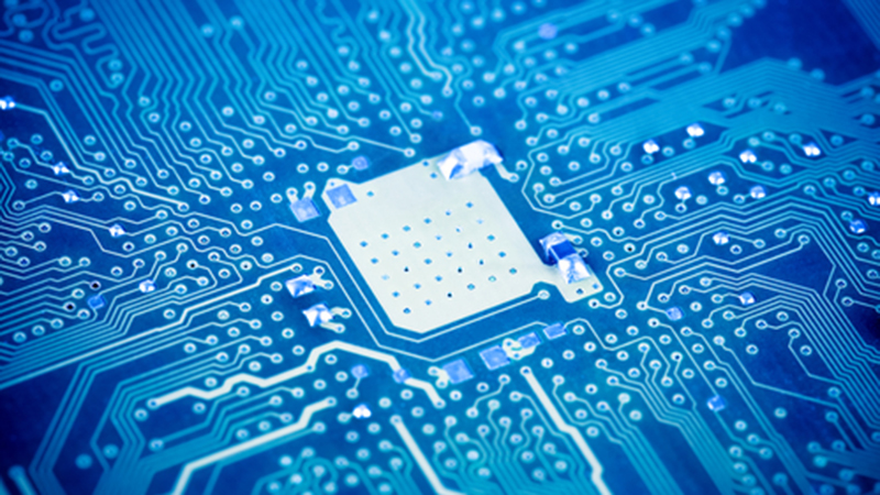
PCB reverse engineering
Is it difficult to reverse engineer the board after it's been removed from the device?
PCB reverse engineering is based on the premise of reverse engineering of existing electronic products and printed circuit boards, using reverse research and development technology, reverse analysis of printed circuit boards, copying original technical documents such as PCB files, BOM files, schematic files, etc. 1:1 restoration with PCB silk screen production files, and then use these technical files and production files to carry out PCB board making, component welding, flying probe testing,d circuit boar debugging, and complete the complete copy of the original circuit board model.
PCB reverse engineering is a reverse research technique. Through a series of reverse research techniques, the PCB design circuit, circuit schematic diagram, and BOM table of an excellent electronic product are obtained through reverse engineering PCB software.
Benefits of PCB Reverse Engineering
Specifically, the benefits of PCB reverse engineering are reflected in the following aspects:
1. From a business perspective
Cloning can help enterprises update quickly and keep up with the latest trends. Quickly complete product releases with minimal development costs. And with the support of today's nearly perfect electronic cloning technology, the product quality has been strongly guaranteed.
2. From the perspective of user experience
High quality and low price are its most notable features and are accepted by the public. It can not only enrich people's life, experience the brand-new feelings brought by fashion and trends, but also earn more profits for enterprises and enhance the competitiveness of enterprises in the industry.
3. For some specific industries or research institutions
Reverse engineering is an effective and necessary means. It can quickly overcome technical barriers, promote the development of empirical research, and narrow the gap with advanced technology in developed countries.
4. From the perspective of reverse engineering technology
Reverse engineering is more complex imitation and copying from time to time. It belongs to the field of reverse research. Secondary development can be carried out by overcoming the original machine technology and mastering its performance and application. That is to improve its function on the basis of fully understanding its schematic diagram. Get the product that suits your needs for less. It can not only avoid "intellectual property rights", but also quickly build a brand, and the development cycle is short, the cost of PCB reverse engineering is low, and the benefits are significant.
5. From the perspective of the overall industry
Conducive to accelerating the development of the entire industry. While cloning technology is developing faster and more perfect, electronic engineers are also actively looking for ways to keep newly developed products competitive in the market for a long time and enhance product differentiation. It promotes research in cutting-edge technologies. On the other hand, it also gives a broader development space for reverse analysis, and brings more opportunities to electronic companies.
HOW TO REVERSE ENGINEER A PCB VIA PROTEL
High Tech PCB Reverse Engineering Services - Printed Circuit Board Manufacturing and PCB Assembly - RayMing
The specific technical steps are as follows:
Step 1: Get a PCB, first record the models, parameters, and positions of all components on the paper, especially the direction of the diodes, transistors, and IC gaps. It is best to take two photos of the component location with a digital camera.
Step 2: Remove the parts and tin from the PAD hole. After cleaning the PCB with alcohol, insert it into the scanner. Then lightly polish the top layer and the bottom layer with water gauze paper until the copper film is shiny, put it into the scanner, start Photoshop, and scan the two layers in color.
Step 3: Adjust the contrast and brightness of the canvas to make the difference between the part with copper film and the part without copper film obvious, and then convert the image below to black and white. Check that the lines are clear. If not, repeat this step. If the image is clear, save it as black and white BMP files TOP BMP and BOT BMP; if there are any errors in the graphics, use Photoshop to repair and correct them.
Step 4: Convert the two BMP format files into PROTEL format files respectively, and transfer the two layers into PROTEL. If the positions of the PAD and VIA after two layers coincide, it means that the previous steps are completed. If there is a disagreement, repeat step 3.
Step 5: Convert the BMP of the TOP layer into a TOP PCB, pay special attention to the conversion to the SILK layer, which is the yellow layer, and then draw a line on the TOP layer to insert the device, as shown in the second step. After removal, delete the SILK layer. Repeat until all layers are painted.
Step 6: Convert TOP PCB and BOT PCB to PROTEL, and it is OK to synthesize a picture.
Step 7: Use a laser printer to print the TOP LAYER and BOTTOM LAYER (1:1 ratio) on the transparent film, then put the film on the PCB and check for errors. If it's correct, it's done.
Factors to Consider When Reverse Engineering a PCB
1. Before PCB reverse engineering, the original template needs to be recorded, so that in the later optimization process, once there is a problem with the processing project, it can be reprocessed. If there is no filing, as long as there is a mistake, the subsequent projects will fail, and the impact will be huge.
2. If there are additional requirements when copying the PCB board, if the component BOM is required, the PCB file must be set according to the standard established at the beginning, so as to avoid errors in the BOM table and affect the use. In addition, pay attention to the polarity of each component when removing the board to prevent mistakes during restoration.

3. Before copying the PCB board, it is necessary to measure and record the size of the PCB board to ensure that the board image scanned by the scanner is consistent with the size of the original PCB, and it is easier to prevent the incompatibility of board movement in the later component installation. Moreover, the image scanned by the scanner must be clear to ensure that it is more convenient to view components in the future.
PCB layout of the power circuit
May 31,2023


Just upload Gerber files, BOM files and design files, and the KINGFORD team will provide a complete quotation within 24h.