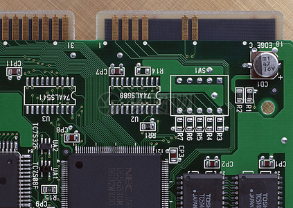
Introductory Tutorial for Multilayer PCB Design
Before designing a multi-layer PCB circuit board, PCB Layout engineers need to determine the circuit board structure used according to the circuit scale, circuit board size and electromagnetic compatibility (EMC) requirements, that is, decide to use 4 layers, 6 layers, Or a circuit board with more layers. Next, let's understand the design steps and precautions of multi-layer PCB boards.
Steps of Multilayer PCB Design
The design process of multilayer PCB circuit board is basically the same as the design steps of ordinary PCB board. Divided into the following steps:
1. The planning of the circuit board is mainly to plan the physical size of the PCB board, the packaging form of the components, the installation method of the components, and the layer structure, that is, single-layer board, double-layer board and multi-layer board.
2. Working parameter setting mainly refers to working environment parameter setting and working layer parameter setting. Correct and reasonable setting of PCB environmental parameters can bring great convenience to the design of circuit boards and improve work efficiency.
3. Component layout and adjustment. After the current work is ready, the netlist can be imported into the PCB, or the netlist can be imported directly by updating the PCB in the schematic diagram. Component layout and adjustment are relatively important tasks in PCB design, which directly affect operations such as subsequent wiring and division of internal electrical layers.
4. The definition and setting of the middle layer of the PCB circuit board. The focus of this operation is to set the specific layer structure in the layer stack manager of the software, mainly to set the number of intermediate signal layers and internal electrical layers, the upper and lower structures, etc.
5. Internal electrical layer segmentation, usually the internal electrical layer, often more than one power network, often needs to divide the internal power layer into several isolated areas, and connect each area to a specific power network, which is a multilayer board The biggest difference from ordinary boards is also an important link in the design of multilayer circuit boards. The structure of the internal electrical layer division often directly affects the routing of the power supply and ground grid, and is also affected by the layout and routing of components.
6. Wiring rule setting is mainly to set various specifications of circuit wiring, wire width, parallel line spacing, safety distance between wires and pads, and via size, etc. No matter what wiring method is adopted, wiring rules are necessary. An indispensable step, good wiring rules can ensure the safety of circuit board wiring, meet the requirements of the manufacturing process, and save costs.
7. Wiring and adjustment. The system provides automatic wiring, but it often cannot meet the requirements of designers. In practical applications, designers often rely on manual wiring, or partially automatic wiring combined with manual interactive wiring to complete the wiring work. Special attention should be paid to the layout and wiring and the characteristics of the internal electrical layer of the PCB circuit board. Although the layout and wiring have a sequence, the layout of the circuit board is often adjusted according to the needs of wiring and internal electrical layer division in the design project, or Adjusting the wiring according to the layout is a process of mutual consideration and mutual adjustment between them.
8. Other auxiliary operations, such as copper plating and teardrop repair, as well as document processing such as report output and save printing. These files can be used to check and modify PCB circuit boards, and can also be used as a list of purchased components.

Considerations for Multilayer PCB Design
When designing high-speed multilayer PCBs, special attention needs to be paid to the design of layers, that is, how you divide signal lines, power lines, ground, and control lines in each layer. The general principle is that the analog signal and the analog signal ground must at least have a separate layer. It is also recommended to use a separate layer for the power supply.
General principles of multi-layer PCB layer layout:
1) The bottom of the device surface (the second layer) is the ground plane, providing the device shielding layer and providing a reference plane for the wiring of the device surface;
2) All signal layers should be adjacent to the ground plane as much as possible;
3) Try to avoid direct adjacency between two signal layers;
4) The main power supply is adjacent to its corresponding ground as much as possible;
5) In principle, a symmetrical structure design should be adopted. The meaning of symmetry includes: dielectric layer thickness and type, copper foil thickness, graphics
6) The symmetry of the distribution type (large copper foil layer, circuit layer).
In some cases, older legacy PCB footprints may not be sufficient for multi-layer designs, so you will need to determine if there are any additional requirements. Depending on the CAD system used, you may have to add layers or attributes to the schematic for multilayer use. Having access to more advanced PCB design systems here with links to online library services would be a real bonus. Using the latest and most accurate PCB footprint source data can be a lot easier.
The main difference between a two-layer and multilayer board setup is planning your layer stackup. Here are some key points to consider when planning your board layer stack-up:
Performance: How fast the circuit will run, and ultimately the operating environment of the board, can affect the material from which the board is made. There are various materials higher than FR-4 that may be better suited for your application depending on your needs, but these may affect parameters such as impedance calculations. Here, the help of your PCB manufacturer will be a valuable source of information.
Cost: The materials of manufacture as well as the number of layers and configuration will directly affect the overall cost of building the board. Here again, you need to consider all options with the manufacturer.
Density: The wiring density of the board is another factor in determining the layer stack configuration of the board. It's a pain when you have to go back and add layers to your board design after you've already started layout. Not only will you need to reconfigure the CAD database, but you may also have to make a lot of changes to the layout. On the other hand, if you're starting with too many layers, then you'll be paying more for the board, then you should.
Circuitry: You also need to understand the needs of the circuit in order to create the best layer configuration. For example, for best performance, sensitive signals may require a stripline layer configuration, which means adding additional ground planes. The analog and digital circuit areas will need to be separated with their own ground planes, and the on-board power supplies will need to be isolated. All of these can affect layer configuration, so this should be planned before layout begins.
Once the data has been collected and the layer stack created in the layout database, board placement and routing can begin.
Using a tool like this board outline generator makes it easier to create board layer stacks
Different perspectives on location and route
One of the first things that differentiates you when working on a multi-layer layout is that you need to start thinking about the "3D" design aspect. Two-layer boards only require you to think about "top" and "bottom". Now you're in a multi-layered world with a lot of different things going on inside that can affect the top and the bottom. For example, you might not want to place a noisy part somewhere due to sensitive routing on the inner layers beneath it.
As far as tooling is concerned, the way components are placed will be the same as on a double-sided board, but the skins used will be different. For example, you don't have to worry about leaving enough space between parts to route since most of them will be routed on internal layers. For sensitive circuits, it is still necessary to use short direct paths on the surface layer, but in most cases you can now use more space. This is also a good thing, because multilayer boards may require more components to be placed.
Internal trace routing and power planes will be interesting, but in the meantime, here are some important considerations:
·
Multi-layer boards will generally have more components and therefore more wiring than double-sided boards, so plan ahead. Depending on the technology of the board, some of these traces may have specific trace width and space or other requirements, such as differential pairs or impedance-controlled traces.
·
·
Some routing will require a stripline layer structure and must be routed on a layer adjacent to the ground plane. In addition, sensitive routing must cross vertically on adjacent internal signal layers to help reduce any possible broadside coupling or crosstalk.
·
·
There will be many vias in the ground plane for connections, but these may interfere with the signal return path. This requires careful planning of your route to avoid blocking the aircraft.
·
·
Split planes need to be laid out so that sensitive signals do not cross the split, disrupting their return path. Such a situation can generate a lot of noise on the board.
·
Once the layout and routing checks are done, the rest of the design work will be similar to double-sided boards. Now you are ready to build the board.
Multilayer PCB layout requires 3D perspective for board design


