About the "Golden Finger" in PCB
1. The definition of gold finger
(Gold Finger or Edge Connector) Insert one end of the PCB board into the connector card slot, use the pins of the connector as the outlet for the external connection of the pcb board, and make the pad or copper contact with the pins at the corresponding position to achieve conduction. For the purpose of communication, and immerse gold or plate nickel gold on this pad or copper skin of the pcb board, because it is in the shape of a finger, it is called a gold finger.

2. The surface treatment method of gold finger PCB
Electroplated nickel gold: the thickness can reach 3-50u", because of its superior electrical conductivity, oxidation resistance and wear resistance, it is widely used on gold finger PCBs that need to be plugged in and out frequently or PCB boards that need to be mechanically rubbed frequently. However, because the cost of gold plating is extremely high, it is only used in local gold plating treatment such as gold fingers. Jeddah PCB is called: selective electro-gold process, the color of electro-gold process is silvery white, not as yellow as immersion gold, the disadvantage is Slightly less weldable.
Figure: Selective electric gold finger PCB (halving tin + gold finger area electric gold)
2. Immersion gold: The thickness is generally 1u", up to 3u", because of its superior conductivity, flatness and solderability, it is widely used in high-precision PCB boards with button positions, bound ICs, BGAs, etc. Gold finger PCBs that do not require high wear resistance can also choose the whole board immersion gold process. The cost of the immersion gold process is much lower than that of the electro-gold process. The color of the immersion gold process is golden yellow.
Figure: full board immersion gold PCB
3. Matters needing attention when designing gold fingers
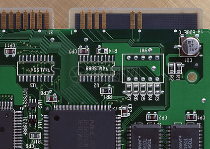
When seeing a shape and package similar to the figure below during PCB design, the first reaction is that there are golden fingers on the board. A relatively simple method for judging cheats: devices with PINs on the TOP and BOTTOM sides of the device; there will be a fool-proof U-shaped groove as shown in the figure below.
When there are gold fingers on the board, it is necessary to do a good job in the details of the gold fingers.
PCB gold finger detail processing:
1) For PCB boards that often need to be plugged and unplugged, in order to increase the wear resistance of the gold fingers, the gold fingers usually need to be electroplated with hard gold.
2) Gold fingers need to be chamfered, usually 45°, other angles such as 20°, 30°, etc. If there is no chamfer in the design, there is a problem; as shown in the figure below, the arrow shows a 45° chamfer:
3) The gold finger needs to be treated with a whole piece of solder mask and window opening, and the PIN does not need to be stenciled;
4) The immersion tin and immersion silver pads need a minimum distance of 14mil from the top of the finger; it is recommended to design
When the pad is more than 1mm away from the finger position, including the via pad;
5) Do not spread copper on the surface of the gold finger;
The following picture shows the design of a golden finger for reference:
6) All layers of the inner layer of the gold finger need to be copper-cut, and the copper-cut width is usually 3mm larger; half-finger copper-cut and whole-finger copper-cut can be done. In the PCIE design, it is also specified that the copper in the gold finger area should be completely cut off;
The impedance of the gold finger will be relatively low. Cutting copper (hollowing out under the finger) can reduce the impedance difference between the gold finger and the impedance line, and it is also good for ESD;
Suggestion: remove all copper under the gold finger pad.
4. Matters needing attention in Jeddobang PCB golden finger processing
1. Plates with a thickness of 1.2-2.4m can be bevelled. Beveled edges cannot be processed outside this plate thickness range.
2. The depth and angle of the hypotenuse are generally between 20-45 degrees by default. There should be sufficient distance between the gold finger and the edge of the board. According to the board thickness or design requirements of different gold finger PCBs, we recommend that the distance between the gold finger and the edge of the board is 0.6-1.5mm during design, so as to avoid damage to the gold when the bevel is used. Fingers, if the distance between the gold finger and the edge of the board is less than 0.6mm, the beveled edge treatment is required, and there is a risk of injury to the gold finger. The following are several common bevel angles and depth diagrams for your reference.
Plate thickness 1.6mm, bevel depth 1.4mm, bevel angle 25 degrees
Plate thickness 1.6mm, bevel depth 1.3mm, bevel angle 25 degrees
Plate thickness 1.8mm, bevel depth 1.8mm bevel angle 20-25 degrees
Plate thickness 1.2mm, bevel depth 0.4mm, bevel angle 45 degrees
Functional use of "Golden Finger"
· "Gold Finger" interconnection point
When the auxiliary PCB (such as a graphics card, memory stick) is connected to the motherboard, it will pass through one of several female slots, such as PCI, ISA or AGP slots, to transmit signals between peripherals or internal cards and the computer.
· Special adapter
"Golden finger" can enhance the function of the motherboard, insert the motherboard through the secondary PCB, such as memory, graphics card, sound card, network card and other card and slot connection parts, can transmit enhanced graphics and high-fidelity sound, because these cards are rare Detached and reattached, "gold fingers" often outlast the cards themselves.
· Golden finger external connection
The peripherals of the computer are connected to the main board through the PCB "golden fingers". Devices such as speakers, subwoofers, scanners, printers and monitors are all inserted into specific slots on the back of the computer, such as HDMI cables or diplay cables, VGA and DVI cables , these slots are in turn connected to the motherboard's PCB.
"Golden Finger" Manufacturability Design
1
"Gold Finger" bevel design
● The safe distance between the “Golden Finger” and the edge of the shape plate is determined according to the thickness of the finished plate and the angle of the hypotenuse of the “Golden Finger” to determine whether it will hurt the “Golden Finger”. The angle of the conventional hypotenuse is 45 degrees;
● If the designed "golden finger" is too close to the edge of the board, in order not to expose the copper, cut the copper according to the following parameters. If you do not want the "golden finger" to be cut short, you can design the safe distance from the edge of the board according to the following parameters.
2
Solder mask layer window design
In order to facilitate card insertion, the "golden fingers" are not soldered, and all windows are opened. If the windows are not opened, there will be soldering ink between the "golden fingers", and the ink will fall off during multiple insertions and removals, resulting in failure. contact with the card slot.
● Open the window in the "gold finger, tin finger" area, which is about 10MIL larger than the edge of the board;
● The solder mask window is 4mil larger than the line on one side, pay attention to the distance between the window and the copper skin around the "gold finger", and the copper should not be exposed, otherwise copper will be removed;
● The via holes within 2MM of the "Golden Finger" are not allowed to open windows.
3
Board corner treatment design
In order to facilitate card insertion, the outline of the "golden finger" position needs to be chamfered. As for the chamfer or rounded corner, it is designed according to personal preference. If the corner of the outline board is not chamfered, the right angle will damage the card slot when plugging and unplugging. result in reduced product reliability.
4
Copper laying design on line layer
In order to facilitate the insertion of cards, it is best not to have a copper-laying design on the "gold finger" area on the outer surface. If two or more are on the same network, the effect of the copper-laying design is that multiples are connected into one piece, and the produced product is not A single "golden finger" will affect the convenience of plugging and unplugging.
5
Long and short "gold finger" design
● The length of the "gold finger" main lead is 40mil, the auxiliary lead is 20mil, the connection point is 6mil, and the distance between the "gold finger" pad and the 20mil lead is 8mil. The distance between the long "golden fingers" is 8mil;
● When the main lead wire enters the board, it needs to be connected with an oblique line, or if there is a large groove next to the "golden finger", the lead wire needs to be made into a rounded corner instead of a right angle.
6
Imposition design
● When the size of the "Gold Finger" board is less than 40*40MM, it must be beveled first and then mill the shape of the veneer. Secondary appearance positioning, and beveled edge front row CNC process on MI, automatic beveled edge must ensure that the width of the "golden finger" is more than 40MM;
● The "gold finger" board adopts an upside-down imposition method so that the "gold finger" faces outward, and the "gold finger" faces inward as much as possible when PNL is assembled, so that it is convenient to add electric gold leads.


