
Professional PCB manufacturing and assembly
Building 6, Zone 3, Yuekang Road,Bao'an District, Shenzhen, China
+86-13410863085Mon.-Sat.08:00-20:00

Reverse technology development of reverse push principle diagram of PCB copy board
In the research of PCB reverse technology, the reverse deduction schematic diagram refers to the deduction of the PCB circuit diagram based on the PCB file diagram or the direct drawing of the PCB circuit diagram according to the actual product, which aims to explain the principle and working condition of the circuit board. Moreover, this circuit diagram is also used to analyze the functional characteristics of the product itself. In the forward design, the research and development of general products should first carry out the schematic diagram design, and then carry out the PCB design according to the schematic diagram.
Whether it is used to analyze the circuit board principle and product operating characteristics in reverse research, or reused as the basis and basis for PCB design in forward design, PCB schematic diagrams have a special role. Then, according to the file diagram or the real object, how to reverse the PCB schematic diagram, and what details should be paid attention to during the reverse derivation process?
When performing reverse design of a schematic diagram of a complete PCB circuit board, a reasonable division of functional areas can help engineers reduce unnecessary troubles and improve the efficiency of drawing. Generally speaking, components with the same function on a PCB board will be arranged in a centralized manner, and dividing the area by function can provide a convenient and accurate basis for reverse derivation of the schematic diagram. However, this division of functional areas is not arbitrary. It requires engineers to have a certain understanding of electronic circuit related knowledge. First, find out the core components in a certain functional unit, and then find out other components of the same functional unit according to the wiring connection to form a functional partition. The formation of functional partitions is the basis of schematic diagram drawing. In addition, in this process, don't forget to make good use of the serial numbers of components on the circuit board, which can help you perform functional partitioning faster.
This reference part can also be said to be the main component PCB copy board used at the beginning of the drawing of the schematic diagram. After the reference part is determined, drawing according to the pins of these reference parts can ensure the accuracy of the schematic diagram to a greater extent. sex. For engineers, the determination of reference parts is not a very complicated matter. Generally, components that play a major role in the circuit can be selected as reference parts. They are generally larger in size and have more pins, which is convenient for drawing. Such as integrated circuits, transformers, transistors, etc., can be used as suitable reference parts.
Correctly distinguish lines and draw wiring reasonably
For the distinction between ground wires, power wires, and signal wires, engineers also need to have relevant power supply knowledge, circuit connection knowledge, PCB layout knowledge, and so on. The distinction of these lines can be analyzed from the aspects of the connection of components, the width of the copper foil of the line, and the characteristics of the electronic product itself. In wiring drawing, in order to avoid crossing and crossing of lines, a large number of grounding symbols can be used for ground lines, different lines of different colors can be used for various lines to ensure clear identification, special signs can be used for various components, and even Draw unit circuits separately and combine them at the end.
Master the basic framework and establish similar principles
Engineers need to be proficient in the frame composition and schematic drawing of some basic electronic circuits, not only to be able to directly draw the basic composition forms of some simple and classic unit circuits, but also to be able to form the overall framework of electronic circuits. On the other hand, don't ignore that the same type of electronic products have a certain similarity in the schematic diagram of the PCB copy board. Engineers can make full use of similar circuit diagrams to reverse the new product schematic diagram based on the accumulation of experience.
After the schematic drawing is completed, the reverse design of the PCB schematic diagram can only be said to be completed after testing and checking. The nominal value of components sensitive to PCB distribution parameters needs to be checked and optimized. According to the PCB file diagram, the schematic diagram is compared, analyzed and checked to ensure that the schematic diagram is completely consistent with the document diagram. If the layout of the schematic diagram is found to be inconsistent with the requirements during the check, the schematic diagram will also be adjusted until it is completely reasonable and standardized, accurate and clear.
Professional touch screen maintenance, inverter maintenance, servo driver maintenance, plc, DC speed controller maintenance, various electrical industrial power supplies, boards, motor maintenance, CNC system maintenance
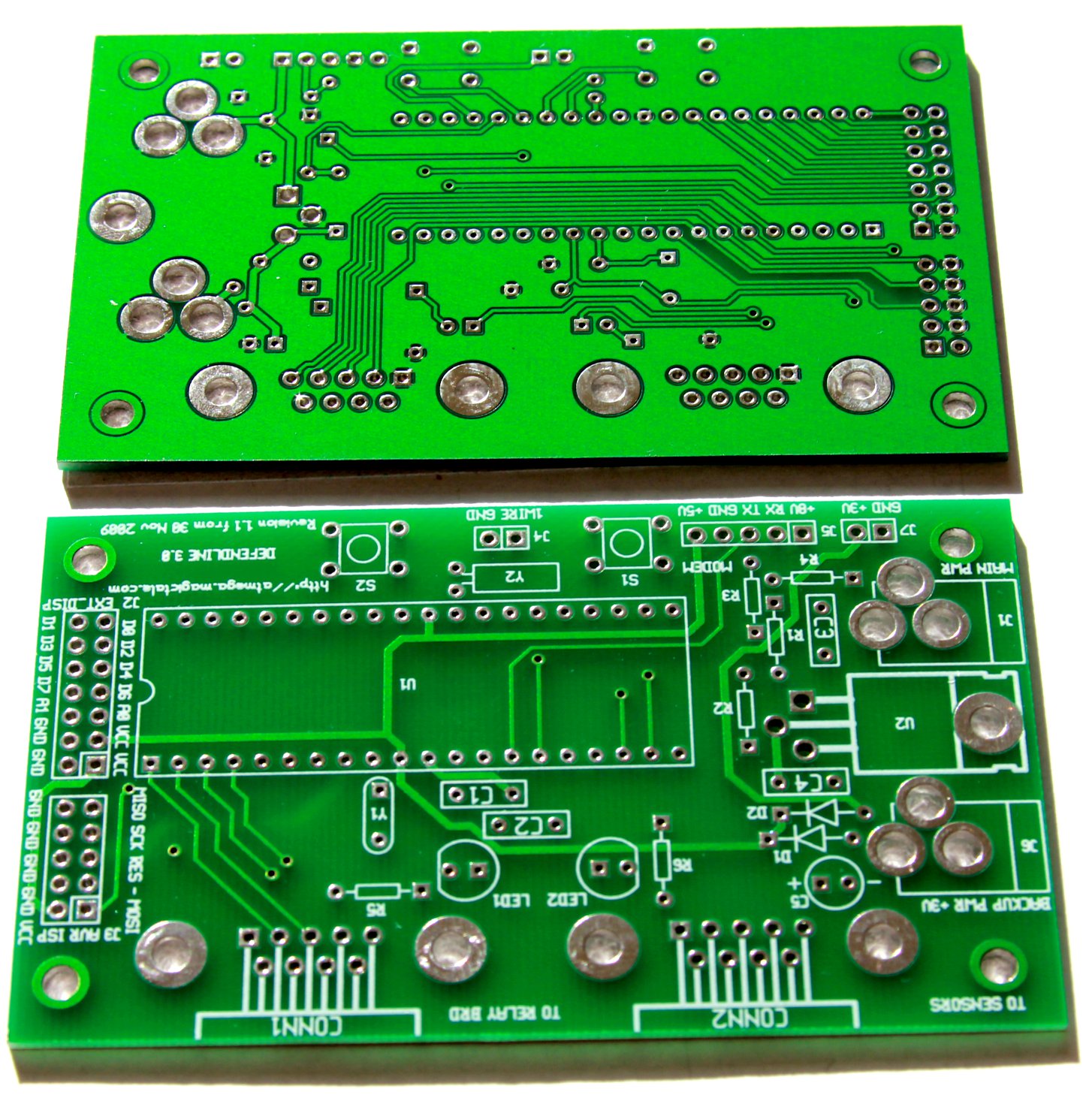
PCB copy board reverse push schematic diagram reverse technology development PCB copy board reverse push schematic diagram reverse technology development PCB copy board, the industry is also often called circuit board copy board, circuit board clone, circuit board copy, PCB clone, PCB reverse Design or PCB reverse development.
That is, on the premise that there are already physical electronic products and circuit boards, reverse analysis of the circuit board is carried out by means of reverse research and development technology, and technical documents such as the PCB file, bill of materials (BOM) file, and schematic file of the original product and PCB silk screen production files are restored 1:1.
Then use these technical documents and production documents to carry out PCB board making, component welding, flying probe testing, circuit board debugging, and complete the complete copy of the original circuit board model.
For PCB copy boards, many people do not understand what is PCB copy boards, and some people even think that PCB copy boards are copycats.
In everyone's understanding, copycat means imitation, but PCB copy board is definitely not imitation. The purpose of PCB copy board is to learn the latest foreign electronic circuit design technology, and then absorb excellent design solutions, and then use it to develop and design better The product.
With the continuous development and deepening of the copy board industry, today's PCB copy board concept has been extended in a wider range, no longer limited to simple circuit board copying and cloning, but also involves the secondary development of products and the development of new products research and development.
For example, through the analysis of existing product technical documents, understanding and discussion of design ideas, structural features, process technology, etc., it can provide feasibility analysis and competitive reference for the development and design of new products, and assist R&D and design units to follow up the latest Technological development trends, timely adjustment and improvement of product design plans, and research and development of new products with the most market competitiveness.
The process of PCB copy board can realize the rapid updating and upgrading and secondary development of various types of electronic products through the extraction and partial modification of technical data files. According to the file diagram and schematic diagram extracted from the copy board, professional designers can Willing to optimize the design and modify the PCB.
It is also possible to add new functions to the product or redesign the functional features on this basis, so that products with new functions will appear at the fastest speed and with a new attitude, not only have their own intellectual property rights, but also in the market Winning the opportunity will bring double benefits to customers.
Whether it is used to analyze the circuit board principle and product operating characteristics in reverse research, or reused as the basis and basis for PCB design in forward design, PCB schematic diagrams have a special role.
Then, according to the file diagram or the real object, how to reverse the PCB schematic diagram, and what is the reverse process like? What details should be paid attention to?
About the "Golden Finger" in PCB
May 31,2023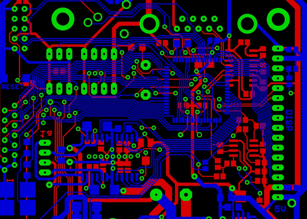


Just upload Gerber files, BOM files and design files, and the KINGFORD team will provide a complete quotation within 24h.